
Single-Stage Amplifier Circuit PCB Design: A Comprehensive Guide
1. Introduction
Printed Circuit Board (PCB) design is a critical aspect of electronic circuit development, especially for analog circuits like single-stage amplifier circuits. A well-designed PCB ensures signal integrity, minimizes noise, and This article provides a detailed guide on designing a PCB for a single-stage (single-transistor) amplifier circuit, covering key considerations such as component placement, routing, grounding, and noise reduction techniques.
2. Overview of Single-Stage Amplifier Circuits
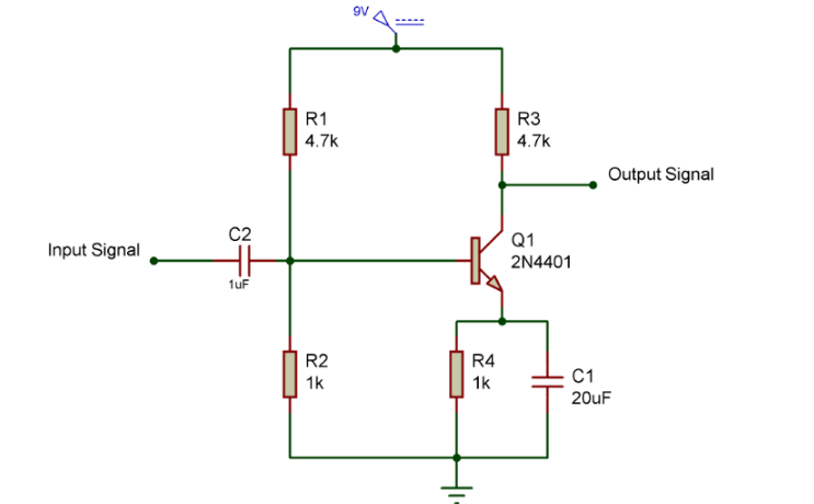
A single-stage amplifier typically consists of a single active device (such as a bipolar junction transistor (BJT) or a field-effect transistor (FET)) configured in common-emitter (for BJT) or common-source (for FET) topology. The basic components include:
- Transistor (BJT/FET) – The amplifying device.
- Biasing resistors – To set the operating point.
- Coupling capacitors – To block DC while allowing AC signals to pass.
- Bypass capacitor – To stabilize the emitter/source voltage.
- Load resistor – To define the gain.
The PCB layout must ensure proper signal flow, minimal parasitic effects, and thermal stability.
3. Key Considerations in PCB Design for Single-Stage Amplifiers
3.1. Component Placement
Proper component placement is crucial for minimizing parasitic capacitance and inductance, which can degrade amplifier performance.
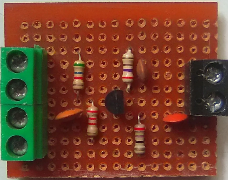
- Place the transistor centrally to minimize trace lengths.
- Keep input and output paths short to reduce noise pickup.
- Position bypass capacitors close to the transistor’s emitter/source terminal to ensure effective AC grounding.
- Arrange biasing resistors near the transistor base/gate to minimize interference.
3.2. Power Supply Decoupling
Noise from the power supply can significantly affect amplifier performance. Use:
- A bulk capacitor (e.g., 10µF electrolytic) near the power entry point.
- A smaller ceramic capacitor (0.1µF) close to the transistor’s collector/drain to filter high-frequency noise.
3.3. Grounding Techniques
A poor grounding scheme can introduce noise and oscillations.
- Use a star-grounding configuration where all ground connections meet at a single point near the power supply.
- Avoid ground loops by ensuring that high-current and low-current grounds are separated.
- Use a ground plane (if designing a 2-layer PCB) to provide a low-impedance return path.
3.4. Signal Routing
- Keep input and output traces short and direct to avoid parasitic capacitance.
- Avoid running high-impedance traces parallel to high-current traces to prevent crosstalk.
- Use wider traces for power lines to reduce resistance and inductance.
3.5. Thermal Management
Transistors dissipate heat, which can affect performance.
- Use adequate copper pours around the transistor to act as a heat sink.
- Ensure proper spacing between heat-generating components.
4. Step-by-Step PCB Design Procedure
4.1. Schematic Design
Before PCB layout, design the circuit schematic using software like KiCad, Altium, or Eagle. Verify the circuit’s functionality through simulation (e.g., LTspice).
4.2. PCB Layout Design
- Define the board dimensions based on the enclosure and component sizes.
- Place the transistor first, followed by biasing components and capacitors.
- Route critical signal paths (input, output, and feedback) with minimal bends.
- Implement power and ground planes (if using a multilayer PCB).
- Add decoupling capacitors near the power pins of active components.
4.3. Design Rule Check (DRC)
Run a DRC to verify:
- Minimum trace width and spacing.
- Proper via sizes.
- Unconnected nets.
4.4. Gerber File Generation
Generate Gerber files for manufacturing, including:
- Copper layers.
- Silkscreen (for component labels).
- Drill files.
5. Common Pitfalls and How to Avoid Them
5.1. Poor Grounding
- Problem: Ground loops or noisy ground paths.
- Solution: Use a star-grounding scheme or a solid ground plane.
5.2. Excessive Trace Lengths
- Problem: Increased parasitic inductance/capacitance.
- Solution: Keep high-frequency traces short and direct.
5.3. Inadequate Decoupling
- Problem: Power supply noise affecting amplifier stability.
- Solution: Place decoupling capacitors as close as possible to the transistor.
5.4. Incorrect Biasing Due to PCB Leakage
- Problem: High-impedance nodes picking up noise.
- Solution: Use guard rings or increase trace separation.
6. Testing and Troubleshooting
After fabrication:
- Check for shorts/open circuits using a multimeter.
- Measure DC bias points to ensure the transistor is operating in the correct region.
- Test frequency response using a signal generator and oscilloscope.
- Look for oscillations (indicative of poor layout or feedback issues).
7. Conclusion
Designing a PCB for a single-stage amplifier requires careful attention to component placement, grounding, decoupling, and signal routing. By following best practices in PCB design, engineers can ensure optimal performance, minimal noise, and reliable operation. Simulation and prototyping are essential steps to validate the design before mass production.
With proper planning and execution, a well-designed PCB can significantly enhance the performance of a single-stage amplifier circuit, making it suitable for applications in audio amplification, RF circuits, and sensor signal conditioning.