Solving Blind Via Issues in PCB Design and Manufacturing
Abstract
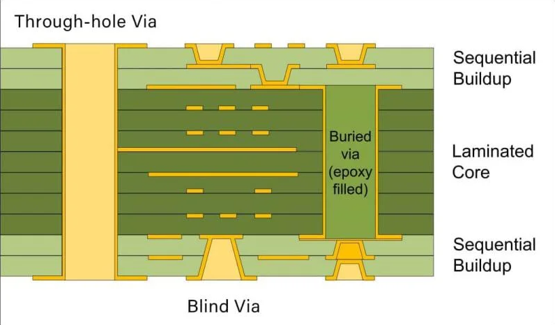
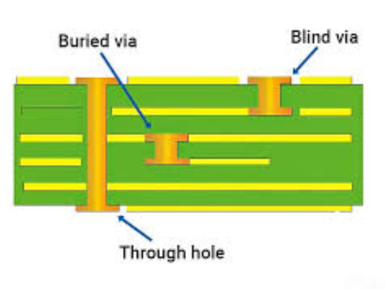
Blind vias are essential in modern high-density printed circuit board (PCB) designs, enabling connections between outer layers and inner layers without penetrating the entire board. However, blind vias present several challenges, including reliability concerns, manufacturing complexities, and signal integrity issues. This paper explores common problems associated with blind vias, analyzes their root causes, and provides practical solutions to enhance PCB performance and manufacturability. Key topics include material selection, drilling techniques, plating quality, and design optimization.
1. Introduction
With the increasing demand for miniaturization and high-speed electronics, multilayer PCBs with blind vias have become a standard in advanced designs. Blind vias allow for higher routing density, reduced layer count, and improved signal performance by minimizing stub effects. However, their implementation introduces challenges such as misalignment, poor plating, and thermal stress failures. Addressing these issues requires a combination of optimized design practices, precise manufacturing techniques, and thorough testing.
2. Common Blind Via Problems and Solutions
2.1. Drilling and Registration Accuracy
Problem: Blind vias require precise depth control during laser or mechanical drilling. Misalignment between layers can lead to open circuits or unreliable connections.
Solutions:
- Use laser drilling for higher precision compared to mechanical drilling.
- Implement optical alignment systems to ensure accurate layer registration.
- Apply step-drilling techniques for deeper blind vias to avoid excessive material removal.
2.2. Plating Uniformity and Void Formation
Problem: Incomplete copper plating inside blind vias can cause weak interconnections or open circuits due to voids.
Solutions:
- Optimize electroplating parameters (current density, bath chemistry) for uniform deposition.
- Use pulse plating to enhance copper filling in high-aspect-ratio vias.
- Implement via filling techniques (conductive or non-conductive pastes) to prevent voids.
2.3. Thermal and Mechanical Stress Failures
Problem: Blind vias are susceptible to cracking under thermal cycling or mechanical stress due to coefficient of thermal expansion (CTE) mismatches.
Solutions:
- Select low-CTE materials (e.g., high-Tg FR4, polyimide) to reduce stress.
- Apply conformal coating or underfill to reinforce via structures.
- Design teardrop-shaped pads to minimize stress concentration.
2.4. Signal Integrity and Impedance Control
Problem: Blind vias can introduce impedance discontinuities, leading to signal reflections and degraded high-frequency performance.
Solutions:
- Use back-drilling to remove unused via stubs.
- Optimize via aspect ratio (depth/diameter) to minimize inductance.
- Implement differential via pairs for high-speed signals to maintain impedance matching.
2.5. Cost and Manufacturing Complexity
Problem: Blind vias increase fabrication costs due to additional drilling and plating steps.
Solutions:
- Use stacked or staggered microvias to reduce layer count while maintaining functionality.
- Adopt HDI (High-Density Interconnect) processes for cost-effective mass production.
- Collaborate with PCB manufacturers early in the design phase to optimize via placement.
3. Advanced Techniques for Blind Via Reliability
3.1. Sequential Lamination
For complex multilayer PCBs, sequential lamination allows blind vias to be formed in separate stages, improving alignment and reliability.
3.2. Via-in-Pad Design
Placing blind vias directly under component pads saves space but requires careful plating and filling to prevent solder wicking.
3.3. Non-Conductive Filling
Filling blind vias with epoxy or resin improves mechanical strength and prevents solder migration during assembly.
4. Testing and Quality Assurance
- Cross-section analysis to inspect plating quality.
- Automated optical inspection (AOI) for detecting misalignment.
- Thermal cycling tests to assess long-term reliability.
5. Conclusion
Blind vias are indispensable for modern PCB designs but require careful consideration of manufacturing and reliability challenges. By optimizing drilling techniques, plating processes, material selection, and design strategies, engineers can mitigate common issues and enhance PCB performance. Future advancements in laser drilling and additive manufacturing may further improve blind via reliability and cost efficiency.