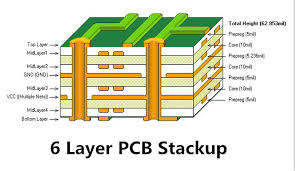
6-Layer PCB Stackup Design for High-Speed Applications
Introduction In today’s rapidly advancing electronics industry, high-speed digital designs have become ubiquitous across various applications including networking equipment, telecommunications, computing systems, and advanced consumer electronics. As signal frequencies continue to increase and rise times decrease, proper printed circuit board (PCB) stackup design has emerged as a critical factor in ensuring signal integrity, power integrity,…