6-Layer PCB Stackup Design for High-Speed Applications
Introduction In today’s rapidly advancing electronics industry, high-speed digital designs have become ubiquitous across various applications including networking equipment, telecommunications,…
Introduction In today’s rapidly advancing electronics industry, high-speed digital designs have become ubiquitous across various applications including networking equipment, telecommunications,…
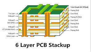
he best practices for 6-layer PCB stacking design include reasonable hierarchy, optimized signal layer layout, good power and grounding design, appropriate use of vias, and effective thermal management. By following these best practices, the performance and reliability of the circuit board can be significantly improved to meet the needs of high-performance applications.
We use cookies to improve your experience on our site. By using our site, you consent to cookies.
Manage your cookie preferences below:
Essential cookies enable basic functions and are necessary for the proper function of the website.
Statistics cookies collect information anonymously. This information helps us understand how visitors use our website.
Google Analytics is a powerful tool that tracks and analyzes website traffic for informed marketing decisions.
Service URL: policies.google.com (opens in a new window)
SourceBuster is used by WooCommerce for order attribution based on user source.
You can find more information in our privacy policy and privacy policy.