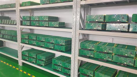
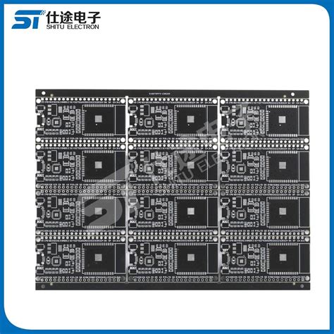
Optimizing PCB Manufacturing: Cost, Quality, and Location
“Strategic PCB manufacturing optimization: balancing cost, quality, and location for seamless prototyping to production with IP safeguards.”
“Strategic PCB manufacturing optimization: balancing cost, quality, and location for seamless prototyping to production with IP safeguards.”
“Explore etching-free PCB creation methods: Discover toner transfer, milling, and UV exposure techniques for precise home fabrication, bypassing traditional etching challenges and fab delays.”
“Find nearby PCB makers offering 24-hour turnaround Get same-day prototypes, competitive pricing, and expert support—avoid 3-week waits with local solutions.”
“Explore top PCB board makers offering low-cost rapid prototyping for 1-5 unit batches. Compare 24-hour turnaround services, design software tips, and budget-friendly small-scale assembly solutions.”
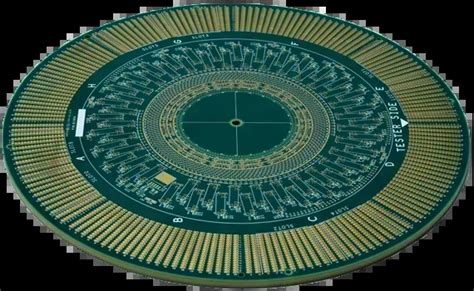
I believe that many people are familiar with PCB circuit boards and may often hear about it in daily life,…
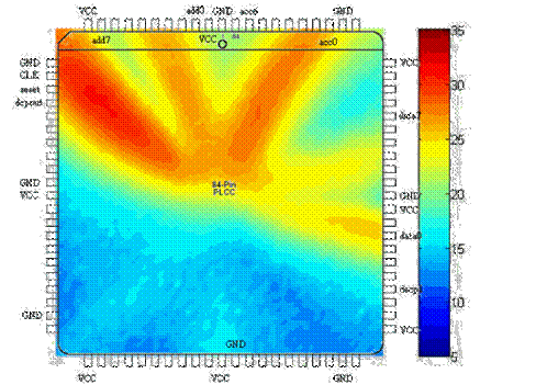
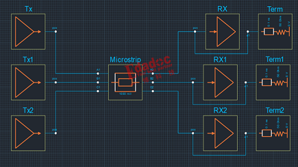
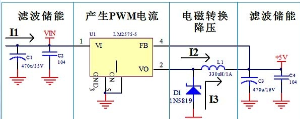
Issues such as spacing, component position, and loop area that should be paid attention to when designing a power supply…

The advantage of high-frequency/microwave/radio frequency PCB board immersion gold process is that the color deposited on the surface is very…

The popularity of handheld wireless communication devices and remote control devices has driven a significant increase in the demand for…
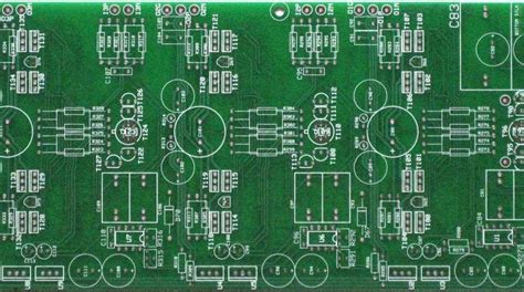
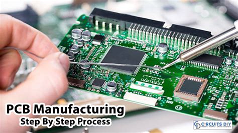
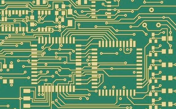
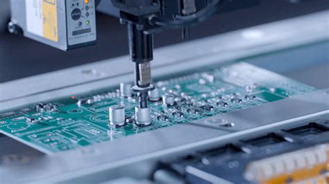
PCB circuit designers need to implement the required functions in PCB circuit design according to the circuit schematic. PCB circuit…
“Discover trusted PC board suppliers merging quality craftsmanship with production expertise. Compare North American innovators offering IP protection and rapid prototyping to global manufacturing solutions balancing cost and precision.”
What are the requirements for PCB design spacing? We will encounter various safety spacing issues in ordinary PCB design, such…
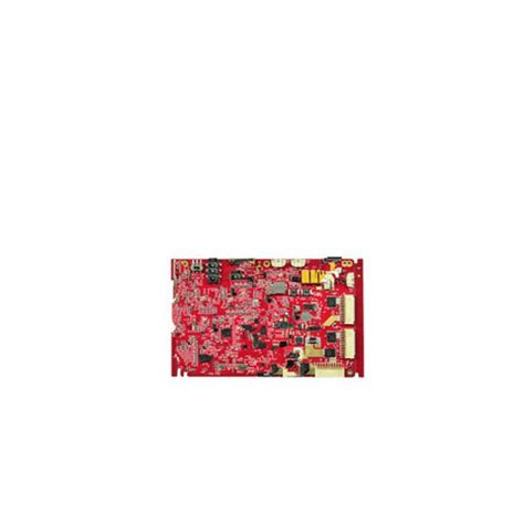
No matter what type of printed circuit board needs to be built, or what type of equipment is used, the…
PCB Layout Some circuit designs are fabricated on tiny silicon wafers, while others consist of various components connected by cables….
1.Function and characteristics Nickel plating is used as the substrate coating of precious metals and base metals on PCB (short…
“Expert PCB manufacturing services from prototyping to full-scale production. Rapid turnaround, certified processes, and DFM optimization ensure precision-engineered boards for your most demanding applications.”
We use cookies to improve your experience on our site. By using our site, you consent to cookies.
Manage your cookie preferences below:
Essential cookies enable basic functions and are necessary for the proper function of the website.
Statistics cookies collect information anonymously. This information helps us understand how visitors use our website.
Google Analytics is a powerful tool that tracks and analyzes website traffic for informed marketing decisions.
Service URL: policies.google.com (opens in a new window)
SourceBuster is used by WooCommerce for order attribution based on user source.
You can find more information in our privacy policy and privacy policy.