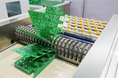
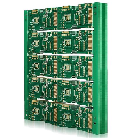
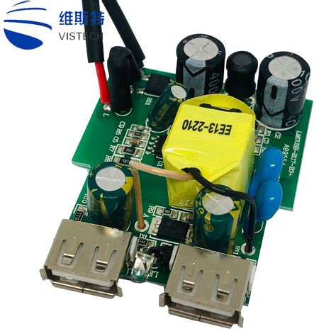
Technical Engineer Shares: Why PCB Design Needs 3D Capabilities?
Designing and building the next generation of electronic products is a complex process, especially in a highly competitive global industry like the electronics industry, where rapid and continuous technological changes have become a common occurrence and the rule of innovation. If designers cannot accept these changes, they will face the risk of being left behind…