Design custom pcb
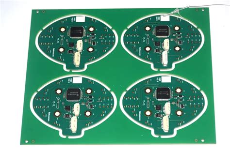
Designing a custom printed circuit board (PCB) is a meticulous process that requires careful planning and execution. The journey begins with a clear understanding of the project requirements, which involves defining the functionality, size, and shape of the PCB. This initial phase is crucial as it sets the foundation for the entire design process. Once the requirements are established, the next step is to create a schematic diagram. This diagram serves as a blueprint, illustrating how different components will be connected. It is essential to ensure that the schematic is accurate and comprehensive, as any errors at this stage can lead to significant issues later on.