Optimizing HDI PCB Layouts for Maximum Density
“Master HDI PCB design optimization with micro via placement, trace width reduction, and IPC-2226 compliance strategies for ultra-compact layouts using advanced EDA tools like Altium Designer.”

“Master HDI PCB design optimization with micro via placement, trace width reduction, and IPC-2226 compliance strategies for ultra-compact layouts using advanced EDA tools like Altium Designer.”
1.Manufacturing technology and structural characteristics HDI board: It is manufactured by build-up method, and the technical level of the board…

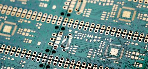
Importance Of HDI In Modern PCB Design High-Density Interconnect (HDI) technology has become a cornerstone in modern printed circuit board…
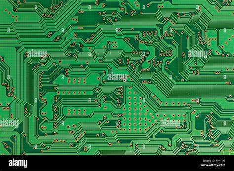
Advantages Of HDI PCB Design In Modern Electronics High-Density Interconnect (HDI) Printed Circuit Board (PCB) design has emerged as a…
We use cookies to improve your experience on our site. By using our site, you consent to cookies.
Manage your cookie preferences below:
Essential cookies enable basic functions and are necessary for the proper function of the website.
Statistics cookies collect information anonymously. This information helps us understand how visitors use our website.
Google Analytics is a powerful tool that tracks and analyzes website traffic for informed marketing decisions.
Service URL: policies.google.com (opens in a new window)
SourceBuster is used by WooCommerce for order attribution based on user source.
You can find more information in our privacy policy and privacy policy.