PCB Footprint Design: A Comprehensive Guide for Engineers
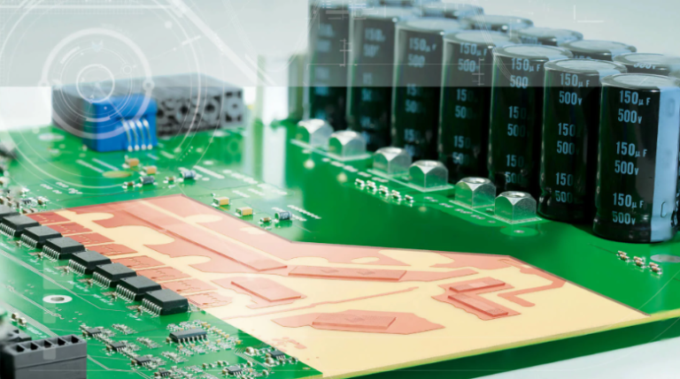
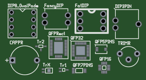
Introduction to PCB Footprints Printed Circuit Board (PCB) footprints, also known as land patterns, are essential elements in electronic design that define the physical interface between a component and the PCB. A footprint specifies the copper pads, solder mask openings, silkscreen outlines, and other features necessary to physically and electrically connect a component to a…