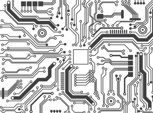
The core of PCB design is to solve problems
0 PCB circuit board design refers to the production of circuit boards by designing schematic drawings and laying out circuits.
Although a perfect PCB design is the best way to avoid problems, it is obviously a temporary solution. For example, if problems are found during the electromagnetic compatibility (EMC) testing phase, it will cause a lot of cost investment, and even the initial design needs to be adjusted and remade, which will take months.
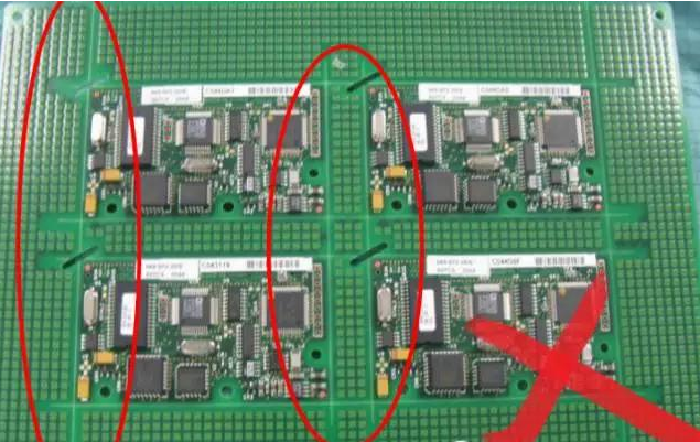
Layout
Layout is the first problem that designers have to face. This problem depends on some of the contents in the drawings, and some devices need to be set together based on logical considerations. However, it should be noted that temperature-sensitive components, such as sensors, should be set separately from heat-generating components including power converters. For designs with multiple power settings, 12-volt and 15-volt power converters can be set in different locations on the circuit board, because the heat and electronic noise they generate will affect the reliability and performance of other components and circuit boards.
In the design process of circuit boards, electromagnetic interference (EMI) is indeed a factor that must be taken seriously. Far-field electromagnetic interference (EMI) problems can be solved by adding filters at noise points or using metal shells to shield signals. However, paying full attention to the devices on the circuit board that can release electromagnetic interference (EMI) allows the circuit board to use a cheaper housing, thereby effectively reducing the cost of the entire system.
In terms of the design of multi-layer circuit boards, the design of through-holes between different circuit board layers is probably the most controversial issue, because through-hole design will bring many problems to the production and manufacturing of circuit boards. Through-holes between circuit board layers will affect the performance of signals and reduce the reliability of circuit board design, so they should be given full attention.
Solution
In the process of PCB circuit board design, many different methods can be used to solve various problems. There are both adjustments to the design scheme itself, such as adjusting the circuit layout to reduce noise; and methods for printed circuit board layout. Design components can be automatically installed through layout tools, but if the automatic layout can be manually adjusted, it will help improve the quality of circuit board design. Through this measure, design rule detection will use technical documents to ensure that the design of the circuit board can meet the requirements of circuit board manufacturers.
Separating different circuit board layers can reduce associated capacitance, but this will increase the number of layers of the circuit board, thereby increasing costs and bringing more problems with through-holes. Although the use of orthogonal power supply system and ground line design may increase the physical size of the circuit board, it can effectively play the role of the ground layer in the double-layer circuit board, reduce the capacitance and complexity of circuit board manufacturing.
Design rule detection is also a very powerful tool that can detect the lines to ensure that the distance between the lines is not too close, which will cause the loop to be too short. However, the overall design still has high economic value. The design planning detection tool can also be used to detect and adjust the power layer and ground layer to avoid large associated capacitance areas.
Conclusion
There are many issues to consider in the design process of printed circuit boards (PCBs), and tools including DesignSpark PCB can effectively handle most of them. By adopting certain best practice guidelines, engineering designers can effectively reduce costs and improve the reliability of circuit boards while meeting system specifications, and bend the system certification at a lower cost to avoid more problems. For more PCB design technology dry goods, please follow the [Quick PCB Academy] official account