
The Surprising Relationship Between PCB Layer Design and Electromagnetic Compatibility (EMC)
Introduction
Printed Circuit Board (PCB) design is a critical aspect of modern electronics, influencing performance, reliability, and manufacturability. However, one often overlooked factor is how PCB layer design directly impacts Electromagnetic Compatibility (EMC)—the ability of a device to function correctly in its electromagnetic environment without introducing intolerable disturbances.
Many engineers focus on component placement and routing but underestimate how layer stackup, grounding strategies, and signal integrity measures affect EMC. Poor PCB layer design can lead to electromagnetic interference (EMI), signal degradation, and even regulatory compliance failures. This article explores the intricate relationship between PCB layer design and EMC, providing insights into optimizing layouts for better electromagnetic performance.
1. Understanding Electromagnetic Compatibility (EMC) in PCBs
EMC ensures that electronic devices:
- Do not emit excessive electromagnetic interference (EMI) that could disrupt nearby systems (emission).
- Are immune to external EMI, maintaining functionality in noisy environments (immunity).
Key EMC challenges in PCBs include:
- Crosstalk (unwanted signal coupling).
- Ground bounce (voltage fluctuations in ground planes).
- Radiated emissions (unintentional RF energy radiation).
- Conducted noise (interference through power and signal lines).
Proper PCB layer design can mitigate these issues by controlling return paths, minimizing loop areas, and reducing parasitic effects.
2. How PCB Layer Stackup Affects EMC
The arrangement of copper layers (stackup) plays a crucial role in EMC performance. A well-designed stackup provides:
- Controlled impedance for high-speed signals.
- Effective shielding against EMI.
- Low-noise power distribution.
Key Stackup Considerations:
A. Number of Layers
- 2-Layer PCBs: Cheaper but offer poor EMC performance due to lack of dedicated ground planes.
- 4-Layer PCBs: A common choice with improved EMC (e.g., Signal-Ground-Power-Signal).
- 6+ Layer PCBs: Best for high-speed designs, allowing dedicated ground/power planes and shielding.
B. Ground and Power Plane Placement
- Adjacent power and ground planes form a natural decoupling capacitor, reducing high-frequency noise.
- Solid ground planes provide low-impedance return paths, minimizing loop area and radiated emissions.
C. Signal Layer Positioning
- High-speed signals should be routed between ground/power planes to contain electromagnetic fields.
- Avoid placing sensitive analog and noisy digital signals on adjacent layers without shielding.
3. Critical PCB Layer Design Techniques for EMC
A. Proper Grounding Strategies
- Single-Point vs. Multi-Point Grounding:
- Single-point is good for low-frequency circuits.
- Multi-point (gridded ground) reduces inductance in high-frequency designs.
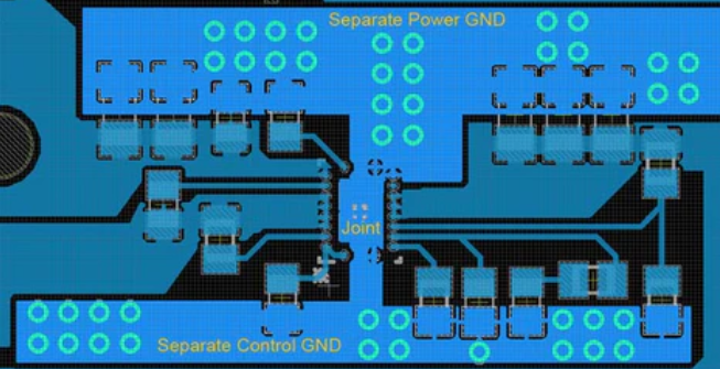
- Split Ground Planes:
- Can help isolate analog and digital grounds but must be connected properly to avoid antenna effects.
B. Minimizing Loop Areas
- Current flows in loops, and larger loops act as antennas, radiating EMI.
- Place signal traces close to their return paths (ground planes) to reduce loop area.
- Use differential signaling for high-speed interfaces (e.g., USB, HDMI) to cancel out EMI.
C. Decoupling and Power Integrity
- Decoupling capacitors should be placed near IC power pins to suppress high-frequency noise.
- Power plane segmentation helps isolate noisy circuits (e.g., switching regulators).
D. Controlled Impedance Routing
- Mismatched impedances cause signal reflections, leading to EMI.
- Use microstrip/stripline configurations with proper dielectric spacing for consistent impedance.
E. Shielding and Partitioning
- Guard traces (grounded copper around sensitive signals) reduce crosstalk.
- Faraday cage techniques (via stitching around high-speed signals) contain EMI.
4. Common PCB Layer Design Mistakes That Harm EMC
A. Insufficient Ground Planes
- A single, fragmented ground plane increases return path impedance, worsening emissions.
B. Poor Return Path Management
- High-speed signals crossing ground plane splits create large loop areas, radiating EMI.
C. Inadequate Power Distribution Network (PDN)
- Thin power traces or insufficient decoupling lead to voltage fluctuations and noise.
D. Ignoring Layer Symmetry
- Asymmetric stackups cause warpage and inconsistent impedance, affecting signal integrity.
E. Overlooking Via Effects
- Long vias introduce inductance, disrupting high-frequency signals and increasing EMI.
5. Practical Tips for EMC-Optimized PCB Layer Design
- Use at least a 4-layer stackup for better EMC performance.
- Route critical signals adjacent to ground planes for controlled impedance.
- Avoid splitting ground planes unless necessary; use a single solid plane if possible.
- Implement proper decoupling with multiple capacitor values for broadband noise suppression.
- Simulate before fabrication using tools like Ansys SIwave or Keysight ADS to predict EMC issues.
6. Case Study: How Layer Design Improved EMC in a High-Speed PCB
A networking device initially failed radiated emissions tests due to excessive noise at 1 GHz. The issues were traced to:
- Poor grounding in the 2-layer design.
- Long, unshielded traces acting as antennas.
Solution:
- Upgraded to a 4-layer stackup (Signal-Ground-Power-Signal).
- Added decoupling capacitors near high-speed ICs.
- Implemented guard traces around clock signals.
Result: Radiated emissions dropped by 15 dB, passing compliance tests.
Conclusion
PCB layer design is a fundamental yet often underestimated factor in achieving good EMC. By optimizing stackup, grounding, power distribution, and signal routing, engineers can significantly reduce EMI and improve device reliability. As electronics continue to shrink and operate at higher frequencies, understanding the interplay between PCB layers and EMC becomes even more critical.
By applying the principles discussed in this article, designers can create PCBs that not only function correctly but also comply with stringent EMC regulations—ensuring robust performance in real-world electromagnetic environments.