
Three wiring skills for PCB high-speed signal circuit design
PCB board design is a compulsory course for electronic engineers, and it is not as easy as it seems to design a perfect PCB board. A perfect PCB board not only needs to have reasonable component selection and setting, but also needs to have good signal conduction performance. This article will introduce and share the wiring skills knowledge in PCB high-speed signal circuit design in detail, hoping to help everyone’s work.
Reasonable use of multilayer boards for PCB wiring
In the actual design process of PCB boards, most engineers will choose to use multilayer boards to complete high-speed signal wiring. This multilayer board is not only an indispensable component, but also an effective means to help engineers reduce circuit interference. When using multilayer boards to complete the high-speed signal circuit design of PCB, engineers need to reasonably choose the number of layers to reduce the size of the printed board, make full use of the middle layer to set up shielding, and achieve nearby grounding, which can effectively reduce parasitic inductance, shorten the signal transmission length, and reduce cross interference between signals. All these methods are very beneficial to the reliability of high-speed circuits.
In addition to the above-mentioned methods of using multilayer boards to improve the reliability of PCB signal transmission, some authoritative data show that the noise of four-layer boards is 20dB lower than that of double-layer boards when the same material is used. The fewer bends in the lead, the better. It is best to use a full straight line. If a turn is required, a 45-degree fold line or arc turn can be used to reduce the external transmission and mutual coupling of high-speed signals, and reduce signal radiation and reflection.
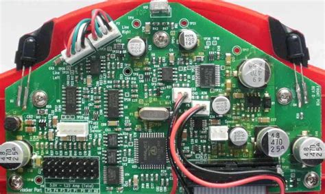
The shorter the lead between the pins of high-speed circuit devices, the better
In the process of designing and wiring PCB high-speed signal circuits, engineers need to shorten the leads between the pins of high-speed circuit devices as much as possible, because the longer the lead, the greater the distributed inductance and distributed capacitance, which will cause reflections and oscillations in the high-speed circuit system.
In addition to shortening the leads between the pins of high-speed circuit components as much as possible, during the PCB wiring process, the fewer the alternations between the lead layers between the pins of each high-speed circuit device, the better, that is, the fewer vias used in the component connection process, the better. Generally speaking, a via can bring about 0.5pF of distributed capacitance, which will significantly increase the delay of the circuit. At the same time, high-speed circuit wiring should pay attention to the “cross interference” introduced by the close parallel routing of signal lines. If parallel distribution cannot be avoided, a large area of ”ground” can be arranged on the reverse side of the parallel signal lines to reduce interference. In two adjacent layers, the routing direction must be perpendicular to each other.
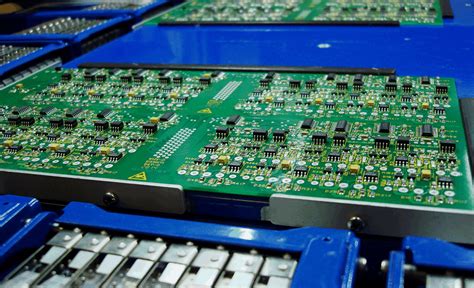
Encircle particularly important signal lines or local units with ground wires
During the wiring design of PCB boards, engineers can use the method of ground wire encirclement for some very important signal lines. They can add protective ground wires to the periphery while routing signals that are not easily interfered with, such as clock signals and high-speed analog signals, and sandwich the signal lines to be protected in the middle. Because in the design process, various signal routing lines cannot form loops, and the ground wires cannot form current loops. If a loop wiring circuit is generated, it will cause great interference in the system. The wiring method of using ground wires to surround signal lines can effectively avoid the formation of loops during wiring. One or more high-frequency decoupling capacitors should be set near each integrated circuit block. When analog ground wires, digital ground wires, etc. are connected to the common ground wire, a high-frequency choke link should be used. Some high-speed signal lines should be specially handled: differential signals are required to be on the same layer and as close to parallel routing as possible. No signal is allowed to be inserted between differential signal lines, and they are required to be of equal length.
In addition to the several design methods mentioned above, when designing PCB signal line routing, engineers should also try to avoid high-speed signal routing branches or stumps. High-frequency signal lines running on the surface are prone to generate large electromagnetic radiation. Routing high-frequency signal lines between the power supply and the ground wire will reduce the radiation generated by the power supply and the bottom layer absorbing electromagnetic waves.