Troubleshooting PCB Component Selection and Drag Issues in Design Software
Introduction
Printed Circuit Board (PCB) design is a complex process that requires precision and attention to detail. One common issue that designers encounter is the inability to select or drag components on the PCB layout. This problem can disrupt workflow, delay projects, and lead to frustration. Understanding the root causes and solutions for this issue is essential for efficient PCB design.
This article explores the reasons why PCB components may not be selectable or draggable in design software such as Altium Designer, KiCad, Eagle, or OrCAD. We will examine software settings, file corruption, layer management, and other factors that contribute to this problem. Additionally, we will provide step-by-step solutions to resolve the issue.
Common Causes of PCB Component Selection and Drag Issues
1. Locked Components
Many PCB design tools allow components to be locked to prevent accidental movement. If a component is locked, it cannot be selected or dragged unless the lock is removed.
Solution:
- In Altium Designer, right-click the component and check Properties to see if the Locked option is enabled. Disable it if necessary.
- In KiCad, select the component and press Ctrl+E to open the properties, then uncheck Locked.
- In Eagle, use the Info tool to check if the component is locked.
2. Incorrect Layer Visibility
PCB designs consist of multiple layers (e.g., Top Layer, Bottom Layer, Silkscreen). If the layer containing the component is hidden, the component may not be selectable.
Solution:
- Open the Layer Settings (or Layer Stack Manager) and ensure that the component’s layer is visible.
- In Altium, press L to open the View Configuration panel and enable all relevant layers.
- In KiCad, use the Layer Manager (hotkey:
Ctrl+L) to adjust visibility.
3. Component is Part of a Group or Union
Some PCB software allows components to be grouped or unionized. If a component is part of a larger group, it may not be individually selectable.
Solution:
- In Altium, use Edit > Select > Inside Area and then Right-Click > Unions > Break All.
- In KiCad, select the group and use Ungroup (if applicable).
- In Eagle, use the Group tool to disband the selection.
4. Design Rules or DRC Restrictions
Design Rule Checks (DRC) can prevent components from being moved if they violate spacing or placement constraints.
Solution:
- Temporarily disable DRC or adjust clearance rules.
- In Altium, go to Design > Rules and modify placement constraints.
- In KiCad, check Design Rules under File > Board Setup.
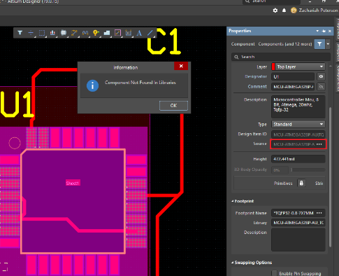
5. Corrupted PCB File or Software Glitch
File corruption or software bugs can cause unexpected behavior, including unresponsive components.
Solution:
- Restart the PCB design software.
- Recover from an earlier backup version.
- Export the design and re-import it into a fresh file.
6. Incorrect Selection Filter Settings
Most PCB design tools have selection filters that control which elements can be selected (e.g., tracks, vias, components).
Solution:
- In Altium, press Shift+F to adjust selection filters.
- In KiCad, check the Selection Filter toolbar.
- In Eagle, ensure that the component layer is selectable in the Options > Set menu.
7. Component is Hidden or Excluded from the Board
Some components may be placed in the schematic but not imported into the PCB layout, making them invisible.
Solution:
- Synchronize the schematic and PCB (Altium: Design > Update PCB).
- In KiCad, use Tools > Update PCB from Schematic.
8. Software-Specific Bugs or Compatibility Issues
Some versions of PCB design software may have bugs that affect component selection.
Solution:
- Update the software to the latest version.
- Check forums or official bug reports for known issues.
Step-by-Step Troubleshooting Guide
If you encounter a PCB component that cannot be selected or dragged, follow these steps:
- Check if the Component is Locked
- Open the component properties and disable the Locked option.
- Verify Layer Visibility
- Ensure the component’s layer is visible in the layer manager.
- Inspect Grouping or Unions
- Break any groups or unions that may restrict movement.
- Disable DRC Temporarily
- Turn off DRC to check if rules are preventing movement.
- Adjust Selection Filters
- Modify selection settings to allow component selection.
- Restart the Software
- Close and reopen the PCB design tool.
- Recover from Backup
- If the file is corrupted, restore from an earlier version.
- Check for Software Updates
- Install the latest patches or updates for the PCB software.
Preventing Future Issues
To avoid PCB component selection problems in the future:
- Avoid Overusing Locks – Only lock critical components.
- Organize Layers Properly – Maintain clear layer visibility settings.
- Regularly Save Backups – Protect against file corruption.
- Keep Software Updated – Ensure compatibility and bug fixes.
Conclusion
The inability to select or drag PCB components can stem from multiple causes, including locked components, layer visibility issues, grouping constraints, or software bugs. By systematically checking each potential issue, designers can quickly resolve the problem and resume their work efficiently.
Understanding these troubleshooting steps ensures smoother PCB design workflows and minimizes disruptions. Whether using Altium, KiCad, Eagle, or another PCB design tool, these solutions provide a structured approach to fixing component selection issues.
By following best practices—such as proper layer management, cautious use of locks, and regular software updates—designers can prevent these issues from recurring and maintain a seamless PCB design process.