
Ultraviolet Lasers in PCB Industry: 4 Major Applications
Introduction
The printed circuit board (PCB) industry has witnessed significant advancements in manufacturing technologies, with ultraviolet (UV) lasers emerging as a critical tool for high-precision processing. UV lasers, typically operating at wavelengths of 355 nm, offer superior beam quality, minimal heat-affected zones (HAZ), and exceptional resolution, making them ideal for PCB fabrication and modification.
This article explores the four major applications of UV lasers in the PCB industry:
- PCB Drilling and Microvia Formation
- Laser Direct Structuring (LDS) and Circuit Patterning
- PCB Cutting and Singulation
- Marking and Engraving for Traceability
Each of these applications leverages the unique advantages of UV lasers to enhance precision, efficiency, and quality in PCB manufacturing.
1. PCB Drilling and Microvia Formation
The Need for Precision Drilling in PCBs
Modern PCBs, especially those used in high-density interconnect (HDI) applications, require extremely small and precise holes for microvias, which facilitate multilayer interconnections. Traditional mechanical drilling struggles with microvia diameters below 100 µm due to tool wear and mechanical stress.
Advantages of UV Lasers in Drilling
- High Precision: UV lasers can produce holes as small as 10–50 µm with exceptional accuracy.
- Minimal Thermal Damage: The short pulse duration reduces heat diffusion, preventing delamination or material warping.
- Non-Contact Process: Eliminates mechanical stress, reducing the risk of cracks or deformations.
Applications in HDI and Flexible PCBs
UV lasers are extensively used in:
- Blind and buried vias for multilayer PCBs
- Flexible PCBs where mechanical drilling may damage thin substrates
- High-frequency PCBs requiring ultra-fine via structures
2. Laser Direct Structuring (LDS) and Circuit Patterning
Challenges in Traditional PCB Patterning
Conventional PCB manufacturing relies on photolithography and chemical etching, which involve multiple steps, mask alignments, and hazardous chemicals. These methods are time-consuming and less adaptable to rapid prototyping.
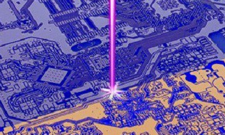
How UV Lasers Enable LDS
UV lasers allow direct writing of circuit patterns on substrates without masks or etching. Key benefits include:
- Maskless Processing: Eliminates photomasks, reducing costs and lead times.
- Fine Line Resolution: Achieves trace widths below 20 µm, essential for miniaturized electronics.
- Material Flexibility: Works on FR4, polyimide, ceramics, and even transparent substrates.
Use Cases in PCB Manufacturing
- Rapid Prototyping: Quick design iterations without retooling.
- High-Density Circuits: Enables finer pitch interconnects in advanced PCBs.
- Additive Manufacturing: Selective laser ablation for conductive traces.
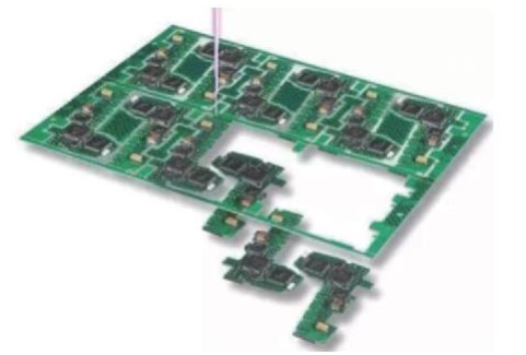
3. PCB Cutting and Singulation
Limitations of Mechanical Cutting
Traditional PCB depaneling methods, such as routing or punching, induce mechanical stress, leading to microcracks, delamination, or solder joint failures—especially in rigid-flex PCBs.
UV Laser Cutting Benefits
- Burr-Free Edges: Produces clean cuts without debris or chipping.
- Complex Geometries: Enables intricate shapes (curves, slots, and cavities).
- No Post-Processing Required: Eliminates the need for deburring or cleaning.
Applications in Advanced PCB Manufacturing
- Rigid-Flex PCBs: Precise cutting without damaging flexible layers.
- Miniaturized Devices: Smartphones, wearables, and IoT modules.
- High-Frequency Boards: Prevents edge roughness affecting signal integrity.
4. Marking and Engraving for Traceability
Importance of PCB Traceability
PCBs require permanent markings for:
- Serial numbers
- Barcodes/QR codes
- Component labels
- Compliance and RoHS markings
Why UV Lasers Excel in PCB Marking
- High Contrast Marks: Produces legible engravings on copper, solder masks, and substrates.
- Non-Destructive: Does not alter electrical properties.
- Permanent and Resistant: Withstands high temperatures, chemicals, and abrasion.
Industry Applications
- Automotive Electronics: Traceability for safety-critical PCBs.
- Medical Devices: FDA-compliant part identification.
- Aerospace and Defense: Tamper-proof markings for security.
Conclusion
UV lasers have revolutionized PCB manufacturing by enabling high-precision, non-contact, and flexible processing. Their four major applications—drilling microvias, direct circuit patterning, depaneling, and marking—address critical challenges in modern electronics, supporting trends like miniaturization, HDI, and rapid prototyping.
As PCB designs continue evolving toward higher complexity and density, UV lasers will remain indispensable in ensuring manufacturing efficiency, reliability, and innovation. Future advancements may include faster pulse rates, hybrid laser systems, and AI-driven laser control for even greater precision.
For PCB manufacturers, investing in UV laser technology is no longer optional—it is a necessity to stay competitive in the fast-paced electronics industry.