
UV lasers in various PCB materials
UV lasers are the best choice for various PCB materials in many industrial fields, from the production of the most basic circuit boards, circuit wiring, to the production of pocket-sized embedded chips and other advanced processes. This material difference makes UV lasers the best choice for various PCB materials in many industrial fields, from the production of the most basic circuit boards, circuit wiring, to the production of pocket-sized embedded chips and other advanced processes.
Application 1: Surface Etching/Circuit Production
UV lasers work quickly when producing circuits, etching surface patterns on circuit boards in minutes. This makes UV lasers the fastest way to produce PCB samples. R&D departments have noticed that more and more sample laboratories are being equipped with in-house UV laser systems.
Depending on optical instrument calibration, the size of UV laser beams can reach 10-20μm, thereby producing flexible circuit traces. The application in Figure 2 shows the biggest advantage of UV in producing circuit traces, which are extremely small and need to be seen under a microscope.
The board measures 0.75″ x 0.5″ and consists of a sintered ceramic substrate and tungsten/nickel/copper/surface. The laser is capable of producing 2-mil circuit traces with 1-mil spacing, resulting in a total spacing of just 3 mils.
While using a laser beam to produce circuits is the fastest way to prototype PCBs, large-scale surface etching applications are best left to chemical processes.
Application 2: PCB Removal
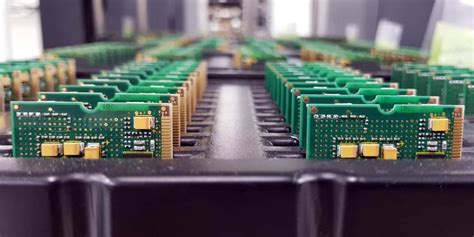
UV laser cutting is an excellent choice for large or small production runs, and is also a good choice for PCB removal, especially when applied to flexible or rigid-flex boards. Removal is the removal of individual boards from the panel, which is a challenge given the increasing flexibility of materials.
Mechanical removal methods such as V-groove cutting and automated board cutting can easily damage sensitive and thin substrates, causing problems for electronic manufacturing service (EMS) companies when removing flexible and rigid-flex boards.
UV laser cutting not only eliminates the effects of mechanical stress during removal, such as edge processing, deformation and damage to circuit components, but also generates less thermal stress than other laser removal applications such as CO2 laser cutting.
The reduction of “cutting buffer” can save space, which means that components can be placed closer to the edge of the circuit, and more circuits can be installed on each circuit board, maximizing efficiency and thus reaching the maximum limit of flexible circuit applications.
Application 3: Drilling
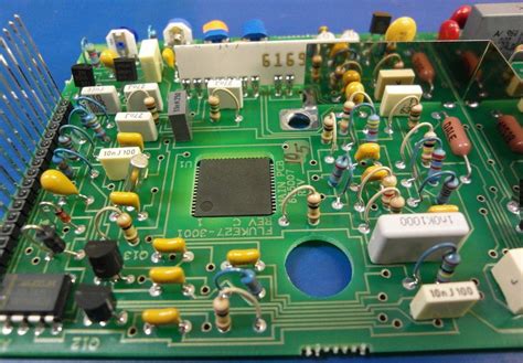
Another application that takes advantage of the small beam size and low stress properties of UV lasers is drilling, including through-holes, microvias and blind and buried vias. UV laser systems drill holes by focusing a vertical beam to cut straight through the substrate. Depending on the materials used, holes as small as 10μm can be drilled.
UV lasers are particularly useful when drilling multiple layers. Multilayer PCBs are heat-pressed together using composite materials. These so-called “semi-cures” can separate, especially after processing with higher-temperature lasers. However, the relatively stress-free properties of UV lasers solve this problem, as shown in Figure 4.
In the cross section shown, a 4-mil diameter hole is drilled through a 14-mil multilayer board. This application, on a flexible polyimide copper-clad substrate, shows no separation between the layers. Another important point about the low-stress properties of UV lasers is that they improve yield figures. Yield is the percentage of usable boards removed from a panel.
UV Laser Applications in Various PCB Materials
During the manufacturing process, many things can cause damage to boards, including broken solder joints, cracked components, or delamination. Any of these factors can cause boards to be thrown into the waste bin on the production line instead of entering a shipping box.
Application 4: Deep Engraving
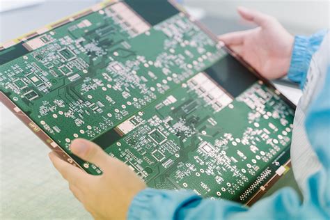
Another application that demonstrates the versatility of UV lasers is deep engraving, which comes in many forms. Using software control of the laser system, the laser beam is set to perform controlled ablation, which is the ability to cut a material to the desired depth, stop, continue, and complete the desired process before moving to another depth and starting another task.
Various depth applications include: small production used when embedding chips and surface grinding to remove organic materials from metal surfaces.
UV lasers can also perform multi-step operations on substrates. On polyethylene, the first step was to create a 2 mil groove with the laser, the second step was to create an 8 mil groove based on the previous step, and the third step was a 10 mil groove. This illustrates the overall user control that UV laser systems provide.
Conclusion: A one-size-fits-all approach
The most striking feature of UV lasers is the ability to complete all of the above applications in a single step. What does this mean for circuit board manufacturing? Instead of using multiple processes and methods on different equipment to complete an application, you can get a complete part in one process.
This streamlined production solution helps eliminate quality control issues when switching boards between processes. UV’s debris-free ablation also means that no post-process cleaning is required.