
What are the skills for high-frequency circuit PCB design
The design of high-frequency circuit PCB is a complex process, and many factors may be directly related to the working performance of high-frequency circuits. High-frequency circuit design and wiring are crucial to the entire design. The following ten skills for high-frequency circuit PCB design are especially recommended:
1.Multilayer board wiring
High-frequency circuits are often highly integrated and have a high wiring density. The use of multilayer boards is both necessary for wiring and an effective means to reduce interference. In the PCB Layout stage, the reasonable selection of the size of a certain number of printed circuit boards can make full use of the middle layer to set up shielding, better achieve local grounding, and effectively reduce parasitic inductance and shorten the transmission length of the signal. At the same time, it can also greatly reduce the cross-interference of the signal, etc. All these methods are beneficial to the reliability of high-frequency circuits. According to data, when the same material is used, the noise of a four-layer board is 20dB lower than that of a double-layer board. However, there is also a problem. The higher the number of PCB half layers, the more complex the manufacturing process and the higher the unit cost. This requires us to select a PCB board with a suitable number of layers when performing PCB Layout. In addition, it is also necessary to carry out reasonable component layout planning and use correct wiring rules to complete the design.
2.The fewer bends in the leads between the pins of high-speed electronic devices, the better
The leads of high-frequency circuit wiring should preferably be all straight lines. If a turn is required, a 45-degree bend or arc turn can be used. This requirement is only used to improve the adhesion strength of copper foil in low-frequency circuits, but in high-frequency circuits, meeting this requirement can reduce the external emission of high-frequency signals and mutual coupling.
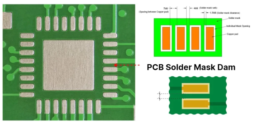
3.The shorter the leads between the pins of high-frequency circuit devices, the better
The radiation intensity of the signal is proportional to the routing length of the signal line. The longer the high-frequency signal lead is, the easier it is to couple to the components close to it. Therefore, for high-frequency signal lines such as signal clocks, crystal oscillators, DDR data, LVDS lines, USB lines, HDMI lines, etc., the shorter the routing is, the better.
4.The fewer interlayer alternations between the leads of high-frequency circuit devices, the better
The so-called “the fewer interlayer alternations of the leads, the better” means that the fewer vias (Via) used in the component connection process, the better. According to the data side, a via can bring about 0.5pF distributed capacitance. Reducing the number of vias can significantly increase the speed and reduce the possibility of data errors.
5.Pay attention to the “crosstalk” introduced by the close parallel routing of signal lines
When wiring high-frequency circuits, pay attention to the “crosstalk” introduced by the close parallel routing of signal lines. Crosstalk refers to the coupling phenomenon between signal lines that are not directly connected. Since high-frequency signals are transmitted along the transmission line in the form of electromagnetic waves, the signal line will act as an antenna, and the energy of the electromagnetic field will be emitted around the transmission line. The unwanted noise signal generated by the mutual coupling of the electromagnetic field between the signals is called crosstalk. The parameters of the PCB board layer, the spacing of the signal lines, the electrical characteristics of the driving end and the receiving end, and the termination method of the signal line all have a certain impact on the crosstalk. Therefore, in order to reduce the crosstalk of high-frequency signals, it is required to do the following as much as possible during wiring:
If the wiring space allows, insert a ground wire or ground plane between the two lines with severe crosstalk, which can play an isolation role and reduce crosstalk. When the space around the signal line itself has a time-varying electromagnetic field, if parallel distribution cannot be avoided, a large area of “ground” can be arranged on the opposite side of the parallel signal line to greatly reduce interference.
Under the premise of wiring space permitting, increase the spacing between adjacent signal lines, reduce the parallel length of the signal line, and try to make the clock line perpendicular to the key signal line instead of parallel. If parallel routing in the same layer is almost unavoidable, the routing directions in two adjacent layers must be perpendicular to each other.
In digital circuits, clock signals are usually signals with fast edge changes and large external crosstalk. Therefore, in the design, the clock line should be surrounded by ground wires and more ground wire holes should be drilled to reduce distributed capacitance, thereby reducing crosstalk. For high-frequency signal clocks, try to use low-voltage differential clock signals and grounding methods, and pay attention to the integrity of the grounding holes.
Do not leave the idle input terminal floating, but connect it to the ground or power supply (the power supply is also the ground in the high-frequency signal loop), because the suspended line may be equivalent to the transmitting antenna, and grounding can suppress the transmission. Practice has proved that this method of eliminating crosstalk can sometimes be effective immediately.
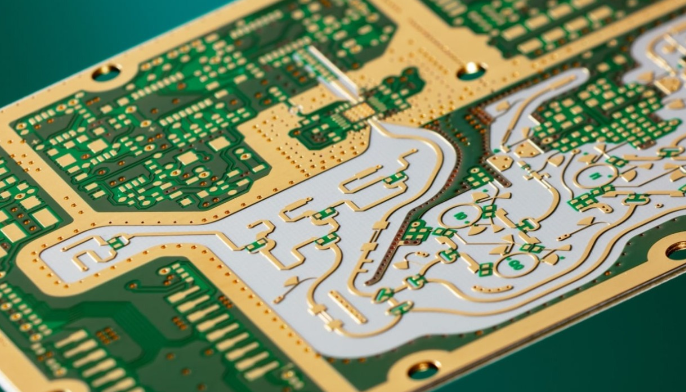
6.Add high-frequency decoupling capacitors to the power pins of integrated circuits
Add a high-frequency decoupling capacitor to the power pins of each integrated circuit. Adding high-frequency decoupling capacitors to the power pins can effectively suppress the interference caused by high-frequency harmonics on the power pins.
7.Isolate the ground wires of high-frequency digital signals and analog signal ground wires
When analog ground wires, digital ground wires, etc. are connected to the common ground wire, they should be connected with high-frequency choke beads or directly isolated and connected at a suitable place. The ground potential of the ground wire of high-frequency digital signals is generally inconsistent, and there is often a certain voltage difference between the two. Moreover, the ground wire of high-frequency digital signals often carries a very rich harmonic component of high-frequency signals. When the digital signal ground wire and the analog signal ground wire are directly connected, the harmonics of the high-frequency signal will interfere with the analog signal through ground coupling. Therefore, under normal circumstances, the ground wires of high-frequency digital signals and analog signals should be isolated. They can be connected at a suitable location by single-point interconnection or by high-frequency choke beads.
8.Avoid loops formed by routing
All kinds of high-frequency signal routing should avoid loops as much as possible. If it cannot be avoided, the loop area should be as small as possible.
9.Good signal impedance matching must be ensured
During the transmission process, when the impedance does not match, the signal will be reflected in the transmission channel. The reflection will cause the synthesized signal to overshoot, causing the signal to fluctuate near the logic threshold.
The fundamental way to eliminate reflection is to make the impedance of the transmission signal well matched. Since the greater the difference between the load impedance and the characteristic impedance of the transmission line, the greater the reflection, the characteristic impedance of the signal transmission line should be equal to the load impedance as much as possible. At the same time, it should be noted that the transmission line on the PCB should not have sudden changes or corners, and the impedance of each point of the transmission line should be kept continuous as much as possible, otherwise reflections will also occur between the sections of the transmission line. This requires that the following wiring rules must be followed when performing high-speed PCB wiring:
USB wiring rules. USB signal differential routing is required, with a line width of 10mil, a line spacing of 6mil, and a ground line and signal line spacing of 6mil.
HDMI wiring rules. HDMI signal differential routing is required, with a line width of 10mil and a line spacing of 6mil. The spacing between each pair of HDMI differential signal pairs exceeds 20mil.
LVDS wiring rules. LVDS signal differential routing is required, with a line width of 7mil and a line spacing of 6mil. The purpose is to control the impedance of HDMI differential signal pairs to 100+-15% ohms
DDR wiring rules. DDR1 routing requires that signals should not pass through holes as much as possible, signal lines should be of equal width, and lines should be equidistant from each other. Routing must meet the 2W principle to reduce crosstalk between signals. For high-speed devices of DDR2 and above, high-frequency data routing is also required to be of equal length to ensure impedance matching of signals.
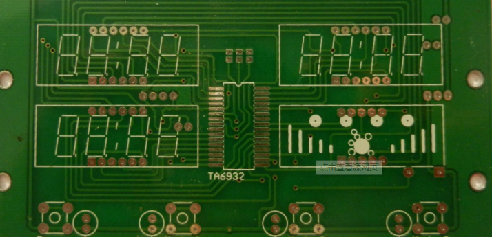
10.Ensure the integrity of transmission
Maintain the integrity of signal transmission and prevent the “ground bounce phenomenon” caused by ground line segmentation.