What is Embedded Resistor and Capacitor (Buried Resistor/Capacitor) Technology?
Introduction to Embedded Passive Components
Modern electronic devices continue to demand higher performance, smaller form factors, and increased functionality. To meet these challenges, the electronics manufacturing industry has developed innovative solutions, among which embedded resistor and capacitor technology—commonly referred to as buried resistor/capacitor or embedded passive technology—has emerged as a critical advancement in printed circuit board (PCB) design and manufacturing.
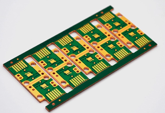
Embedded passive technology involves incorporating resistive and capacitive elements directly within the multilayer structure of a PCB, rather than mounting discrete components on the surface. This approach offers numerous advantages in terms of space savings, electrical performance, reliability, and manufacturing efficiency.
Historical Development of Embedded Passives
The concept of embedded passives isn’t entirely new. The technology traces its roots back to the thick-film hybrid circuits of the 1960s and 1970s, where resistors were screen-printed onto ceramic substrates. However, the modern implementation in organic PCB materials began gaining serious attention in the 1990s as electronic devices became more compact and complex.
The early 2000s saw significant development efforts from major PCB material suppliers and OEMs, with the technology initially finding adoption in high-reliability military and aerospace applications before trickling down to commercial products. Today, as consumer electronics push the boundaries of miniaturization (particularly with the advent of wearables and IoT devices), embedded resistor and capacitor technology has become increasingly relevant.
Embedded Resistor Technology
Materials and Construction
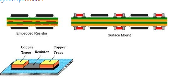
Embedded resistors are typically created using specially formulated resistive materials that are incorporated into the PCB fabrication process. These materials generally fall into three categories:
- Resistive Foils: Thin sheets of nickel-phosphorus (NiP) or similar alloys laminated between dielectric layers
- Polymeric Thick Films (PTF): Polymer-based inks containing conductive particles (usually carbon or silver) screen-printed onto substrate layers
- Ceramic-Based Composites: Mixtures of ceramic and conductive materials offering better stability
The most common approach uses nickel-phosphorus alloys, which can be precisely laser-trimmed to achieve the desired resistance values. These materials typically offer sheet resistances ranging from 10 to 100 ohms per square, allowing for a wide range of resistor values in practical applications.
Fabrication Process
The manufacturing process for embedded resistors generally follows these steps:
- Material Lamination: The resistive material is laminated onto a core substrate or dielectric layer
- Patterning: The resistive layer is patterned using photolithography or laser ablation to create resistor geometries
- Trimming: Laser trimming adjusts the resistor values with high precision (often ±1% or better)
- Overlayering: Additional dielectric layers are applied to bury the resistors within the board structure
- Via Formation: Interconnections are created to connect the embedded resistors to other circuit elements
Advantages of Embedded Resistors
- Space Savings: Eliminates surface-mounted devices (SMDs), freeing up board real estate
- Improved High-Frequency Performance: Reduces parasitic inductance associated with discrete components
- Enhanced Reliability: Fewer solder joints means fewer potential failure points
- Better Thermal Management: Heat dissipation through the entire PCB structure
- Design Flexibility: Allows for more creative component placement and routing
Embedded Capacitor Technology
Materials and Construction
Embedded capacitors utilize high-dielectric-constant (high-k) materials to create capacitive structures within the PCB stackup. Common dielectric materials include:
- Epoxy-Barium Titanate Composites: Polymer-ceramic blends offering moderate capacitance density
- Pure Ceramic Thin Films: Higher performance but more challenging to process
- Nanocomposite Materials: Emerging solutions with tailored dielectric properties
These materials typically provide capacitance densities ranging from 0.5 to 50 nF/cm², sufficient for decoupling and many filtering applications.
Fabrication Process
The creation of embedded capacitors involves:
- Dielectric Material Application: High-k material is coated or laminated onto a conductive plane
- Top Electrode Formation: A second conductive layer is applied to complete the parallel-plate structure
- Patterning: The capacitor structures are defined through etching or laser ablation
- Integration: Additional PCB layers are built up around the capacitor structures
- Interconnection: Vias and plated through-holes connect the capacitors to the appropriate nodes
Advantages of Embedded Capacitors
- Reduced Parasitics: Minimizes equivalent series inductance (ESL) for better high-frequency performance
- Improved Power Integrity: Provides distributed decoupling close to IC power pins
- Board Space Optimization: Eliminates discrete capacitors from the surface
- Enhanced Signal Integrity: Reduces simultaneous switching noise (SSN)
- Manufacturing Efficiency: Reduces component placement and soldering steps
Design Considerations for Embedded Passives
Implementing buried resistor and capacitor technology requires careful design planning:
Resistor Design Factors
- Tolerance Management: While laser trimming can achieve tight tolerances, designers must account for thermal coefficient of resistance (TCR) effects
- Power Handling: Current density and thermal dissipation must be carefully calculated
- Voltage Limitations: Thin resistive materials may have voltage breakdown constraints
- Termination Effects: The interface between resistive material and copper conductors affects performance
Capacitor Design Factors
- Capacitance Density: Limited by available dielectric materials
- Voltage Rating: Thinner dielectrics may limit operating voltage
- Dielectric Loss: Important for high-frequency applications
- Temperature Stability: Some materials exhibit significant capacitance variation with temperature
General Design Guidelines
- Layer Planning: Optimal placement within the layer stackup for performance and manufacturability
- Thermal Considerations: Heat dissipation paths for power components
- Testability: Incorporation of test points for verification
- Design Rules: Specific to the manufacturer’s capabilities
- Modeling Accuracy: Need for precise electromagnetic simulation models
Manufacturing Challenges and Solutions
While embedded passive technology offers significant benefits, it presents several manufacturing challenges:
Process Control
- Material Consistency: Requires tight control over material properties
- Registration Accuracy: Critical for multilayer alignment
- Laser Trimming Precision: Essential for resistor value accuracy
Yield Management
- Defect Detection: Challenges in inspecting buried components
- Repair Limitations: Difficult or impossible to rework embedded components
- Process Optimization: Balancing cost and performance
Cost Considerations
- Material Costs: Specialty materials often carry premium pricing
- Equipment Requirements: Laser trimming and precision deposition systems add capital costs
- Yield Impact: Lower yields can increase effective costs
Manufacturers address these challenges through advanced process controls, statistical process monitoring, and close collaboration with material suppliers.
Applications of Embedded Resistor/Capacitor Technology
High-Frequency Circuits
- RF/Microwave Systems: Improved impedance matching and reduced parasitics
- High-Speed Digital: Better signal integrity for multi-gigabit interfaces
Miniaturized Electronics
- Wearable Devices: Space-constrained form factors
- Medical Implants: Reliability and size requirements
- IoT Sensors: Small footprint and low-power needs
High-Reliability Systems
- Aerospace/Avionics: Reduced failure points for critical systems
- Automotive Electronics: Vibration resistance and thermal performance
- Military Hardware: Ruggedized requirements
Advanced Packaging
- System-in-Package (SiP): Enables higher integration
- 3D IC Integration: Supports vertical stacking approaches
Future Trends in Embedded Passive Technology
The embedded resistor and capacitor field continues to evolve with several promising developments:
Advanced Materials
- Nanocomposites: Tailored electrical properties through nanoscale engineering
- 2D Materials: Graphene and other novel materials offering unique characteristics
- Low-Loss Dielectrics: Improved high-frequency performance
Manufacturing Innovations
- Additive Processes: 3D printing of passive components
- Hybrid Approaches: Combining different material systems
- AI-Optimized Designs: Machine learning for component placement and sizing
Integration Trends
- Higher Densities: More passive components per unit area
- Active-Passive Integration: Combining embedded actives and passives
- Heterogeneous Integration: Mixing different technology nodes and functions
Conclusion
Embedded resistor and capacitor technology represents a significant advancement in electronic packaging, offering substantial benefits in miniaturization, performance, and reliability. While the technology presents certain design and manufacturing challenges, ongoing material developments and process improvements continue to expand its applicability across various market segments.
As electronic devices push toward higher frequencies, greater functionality, and smaller form factors, buried passive technology will play an increasingly important role in enabling these advancements. Designers and manufacturers who master this technology will gain competitive advantages in developing next-generation electronic products.
The implementation of embedded passives requires close collaboration between design engineers, PCB manufacturers, and material suppliers to fully realize the technology’s potential. With proper application, this technology can provide solutions to many of the challenges facing modern electronic system design.