
Why Hole Deviation in PCB Manufacturing Easily Leads to Board Scrapping
Introduction
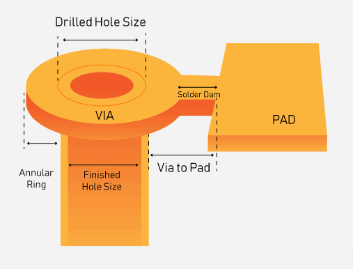
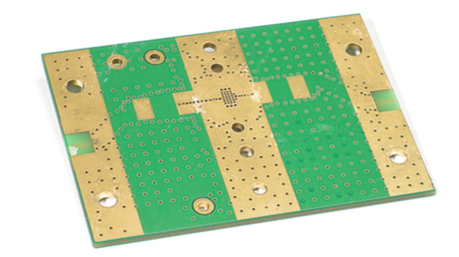
Printed Circuit Boards (PCBs) are the backbone of modern electronics, providing mechanical support and electrical connections for components. One of the most critical processes in PCB manufacturing is drilling, which creates vias and through-holes for component mounting and electrical interconnection. However, even minor deviations in hole positioning—known as hole deviation or hole misregistration—can lead to catastrophic failures, rendering the entire board unusable. This article explores why hole deviation is such a critical issue in PCB manufacturing and why it often results in scrapped boards.
1. The Role of Drilled Holes in PCBs
Before delving into the causes and consequences of hole deviation, it’s essential to understand the functions of drilled holes in PCBs:
- Through-Holes: Used for mounting through-hole components (e.g., resistors, capacitors, connectors).
- Vias: Provide electrical connections between different layers in multilayer PCBs.
- Mounting Holes: Used for securing the PCB to enclosures or heat sinks.
Any misalignment in these holes can disrupt functionality, assembly, or reliability.
2. Causes of Hole Deviation in PCB Manufacturing
Hole deviation occurs when the actual drilled hole position does not match the intended design coordinates. Several factors contribute to this problem:
2.1. Drilling Machine Inaccuracy
- Mechanical Wear: Over time, drill spindles and bearings wear out, leading to positional inaccuracies.
- Tool Deflection: High-speed drilling can cause drill bits to bend, especially with small-diameter drills.
- Machine Calibration Errors: Improper calibration of CNC drilling machines can introduce systematic errors.
2.2. Material-Related Issues
- Laminate Movement: PCB substrates (e.g., FR-4) can expand or contract due to temperature and humidity changes, altering hole positions.
- Inner Layer Misregistration: In multilayer PCBs, slight shifts in inner layer alignment can compound drilling errors.
2.3. Human and Process Errors
- Incorrect Data Input: Errors in CAD/CAM file conversion or drill file generation can lead to misplaced holes.
- Poor Fixturing: Improper PCB clamping during drilling can cause movement, resulting in misaligned holes.
3. Why Hole Deviation Leads to PCB Scrapping
Even small deviations (as little as 0.05 mm) can cause significant problems, often making PCBs unusable. Below are the key reasons why hole misregistration leads to scrapping:
3.1. Component Assembly Failures
- Through-Hole Component Insertion Issues: If holes are misaligned, leads from resistors, capacitors, or connectors may not fit, requiring excessive force that damages pads or traces.
- Surface-Mount Device (SMD) Misalignment: Some SMD components rely on via positions for alignment; deviations can cause soldering defects.
3.2. Electrical Connectivity Problems
- Broken or Weak Connections: If a via is misaligned, it may not properly connect to internal layers, leading to open circuits or intermittent failures.
- Impedance Mismatch: High-frequency PCBs require precise via positioning; deviations can alter signal integrity, causing reflections or crosstalk.
3.3. Mechanical Fit Issues
- Mounting Hole Misalignment: If holes for screws or standoffs are off-position, the PCB may not fit into its enclosure, requiring rework or replacement.
- Press-Fit Connector Failures: Connectors that rely on tight tolerances may not seat correctly, leading to poor electrical contact.
3.4. Rework Challenges
- Difficulty in Repairing: Unlike soldering defects, hole misregistration is often impossible to correct without remanufacturing the board.
- Increased Costs: Scrapping and reworking defective boards lead to material waste and production delays.
4. Industry Standards and Acceptable Tolerances
To minimize hole deviation, PCB manufacturers follow industry standards such as:
- IPC-6012: Defines acceptability criteria for rigid PCBs, including hole positional tolerance.
- IPC-A-600: Provides visual guidelines for PCB inspection.
Typical acceptable hole positional tolerance ranges from ±0.075 mm to ±0.15 mm, depending on the PCB class (Class 1, 2, or 3). Beyond these limits, the risk of failure increases significantly.
5. Mitigation Strategies
To reduce hole deviation and minimize scrapping, PCB manufacturers implement several best practices:
5.1. Advanced Drilling Technologies
- Laser Drilling: Offers higher precision for microvias.
- Automated Optical Inspection (AOI): Detects misalignment before further processing.
5.2. Process Control Improvements
- Regular Machine Maintenance: Ensures drill spindles and positioning systems remain accurate.
- Environmental Control: Maintains stable temperature and humidity to prevent material movement.
5.3. Design for Manufacturability (DFM)
- Adequate Tolerancing: Engineers should account for manufacturing variability in their designs.
- Use of Fiducial Marks: Helps align drilling and assembly processes accurately.
6. Conclusion
Hole deviation in PCB manufacturing is a critical issue that frequently leads to board scrapping due to its impact on assembly, electrical performance, and mechanical fit. Given the high precision required in modern electronics, even minor misalignments can render a PCB unusable. By understanding the root causes—such as machine inaccuracy, material shifts, and process errors—manufacturers can implement better controls, reduce waste, and improve yield. Investing in advanced drilling technologies, stringent process controls, and robust DFM practices is essential to minimizing hole deviation and ensuring high-quality PCB production.
Key Takeaways:
- Hole misregistration is a leading cause of PCB scrapping.
- Even small deviations can disrupt assembly, electrical connections, and mechanical fit.
- Strict process controls and advanced drilling techniques help mitigate the problem.
- Designers and manufacturers must collaborate to optimize tolerances and reduce waste.
By addressing these challenges, the PCB industry can enhance reliability, reduce costs, and deliver higher-quality products to the electronics market.