
4-Layer PCBs: A Comprehensive Guide to Design, Benefits, and Applications
Introduction
Printed circuit boards (PCBs) are the foundation of modern electronics, providing the physical platform for interconnecting electronic components. As electronic devices become more complex and compact, the demand for multi-layer PCBs has grown significantly. Among these, 4-layer PCBs have emerged as a popular choice for a wide range of applications, offering an optimal balance of performance, cost, and design flexibility. This article provides a comprehensive overview of 4-layer PCBs, including their structure, design considerations, advantages, and applications.
What is a 4-Layer PCB?
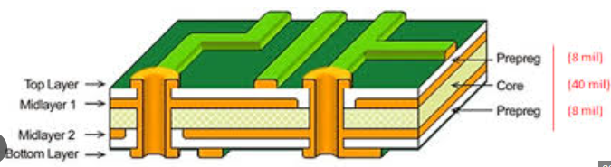
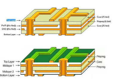
A 4-layer PCB is a type of multi-layer PCB that consists of four conductive copper layers separated by insulating dielectric material. These layers are laminated together to form a single board, with each layer serving a specific purpose. The typical layer stack-up of a 4-layer PCB is as follows:
- Top Layer (Layer 1): The outermost layer, used for component placement and signal routing.
- Inner Layer 1 (Layer 2): Often used as a ground plane to provide a low-impedance return path for signals and reduce electromagnetic interference (EMI).
- Inner Layer 2 (Layer 3): Often used as a power plane to distribute power to components and reduce voltage drops.
- Bottom Layer (Layer 4): The outermost layer, used for additional component placement and signal routing.
The use of dedicated ground and power planes in 4-layer PCBs provides significant advantages in terms of signal integrity, power distribution, and thermal management compared to simpler 2-layer designs.
Design Considerations for 4-Layer PCBs
Designing a 4-layer PCB requires careful planning and attention to detail to ensure optimal performance and manufacturability. Below are some key considerations:
- Layer Stack-Up
The arrangement of layers in a 4-layer PCB is critical to its performance. A common stack-up is:
- Top Layer (Signal)
- Ground Plane
- Power Plane
- Bottom Layer (Signal) This configuration provides excellent signal integrity and EMI shielding. However, the stack-up can be customized based on specific design requirements.
- Signal Integrity
High-speed signals require controlled impedance routing to minimize reflections and losses. The use of ground and power planes in 4-layer PCBs helps maintain consistent impedance and reduces crosstalk between signals. - Power Distribution
Dedicated power planes ensure stable and efficient power delivery to components. Decoupling capacitors should be placed close to power pins to minimize noise and voltage fluctuations. - Thermal Management
The additional layers in a 4-layer PCB provide better thermal conductivity compared to 2-layer designs. Thermal vias can be used to transfer heat from components to the inner layers or external heat sinks. - Routing and Placement
Components should be placed strategically to minimize trace lengths and reduce signal delays. High-speed signals should be routed on the outer layers to avoid interference from the inner planes. - Manufacturing Constraints
Designers must consider manufacturing tolerances, such as minimum trace width, spacing, and via size, to ensure the PCB can be fabricated reliably.
Advantages of 4-Layer PCBs
4-layer PCBs offer several advantages over simpler 2-layer designs, making them suitable for a wide range of applications. Some of the key benefits include:
- Improved Signal Integrity
The use of dedicated ground and power planes reduces noise, crosstalk, and signal reflections, ensuring reliable high-speed performance. - Better Power Distribution
Power planes provide low-impedance paths for power delivery, reducing voltage drops and improving efficiency. - Enhanced EMI Shielding
The ground plane acts as a shield, reducing electromagnetic interference and improving compliance with regulatory standards. - Compact Design
The additional layers allow for more efficient routing and component placement, enabling smaller and more compact designs. - Thermal Performance
The increased thermal conductivity of 4-layer PCBs helps dissipate heat more effectively, improving reliability and lifespan. - Cost-Effectiveness
While 4-layer PCBs are more expensive than 2-layer designs, they offer a cost-effective solution for applications requiring higher performance and complexity.
Applications of 4-Layer PCBs
4-layer PCBs are used in a wide range of applications across various industries. Some of the most common applications include:
- Consumer Electronics
Devices such as smartphones, tablets, and laptops use 4-layer PCBs to accommodate high-speed interfaces, compact designs, and efficient power management. - Telecommunications
Networking equipment, routers, and modems rely on 4-layer PCBs for high-speed data transmission and signal integrity. - Automotive Electronics
Advanced driver-assistance systems (ADAS), infotainment systems, and engine control units (ECUs) use 4-layer PCBs to meet the demanding requirements of automotive environments. - Industrial Automation
Control systems, sensors, and robotics use 4-layer PCBs for reliable performance in harsh industrial conditions. - Medical Devices
Medical imaging systems, diagnostic equipment, and wearable devices use 4-layer PCBs for high-speed data processing and compact designs. - Aerospace and Defense
Avionics, radar systems, and satellite communication equipment use 4-layer PCBs for their reliability and performance in extreme conditions.
Design Workflow for 4-Layer PCBs
The design process for a 4-layer PCB involves several steps, each critical to ensuring a successful outcome. Below is an overview of the typical workflow:
- Schematic Design
The process begins with the creation of a schematic diagram, which defines the electrical connections between components. - Component Placement
Components are placed on the PCB layout, considering factors such as signal integrity, thermal management, and manufacturability. - Layer Stack-Up Definition
The layer stack-up is defined, specifying the arrangement of signal, ground, and power layers. - Routing
Traces are routed on the PCB, with high-speed signals prioritized for controlled impedance routing. Ground and power planes are connected using vias. - Design Rule Check (DRC)
The design is checked against manufacturing and electrical rules to ensure compliance and identify potential issues. - Simulation and Analysis
Signal integrity, power integrity, and thermal performance are simulated and analyzed to optimize the design. - Fabrication and Assembly
The design files are sent to a PCB manufacturer for fabrication. Components are then assembled onto the board using surface-mount technology (SMT) or through-hole technology (THT). - Testing and Validation
The assembled PCB is tested to ensure it meets the required performance and reliability standards.
Future Trends in 4-Layer PCBs
As technology continues to evolve, several trends are shaping the future of 4-layer PCBs:
- Higher Performance Materials
The development of advanced materials with lower dielectric loss and higher thermal conductivity will enable even better performance for 4-layer PCBs. - Miniaturization
The trend toward smaller and more compact devices will drive the need for more efficient routing and component placement in 4-layer designs. - Integration with Advanced Technologies
4-layer PCBs will play a key role in enabling emerging technologies such as 5G, IoT, and artificial intelligence. - Sustainability
The electronics industry is increasingly focusing on sustainable practices, including the use of eco-friendly materials and energy-efficient designs for 4-layer PCBs.
Conclusion
4-layer PCBs have become an essential component of modern electronics, offering a balance of performance, cost, and design flexibility. Their ability to improve signal integrity, power distribution, and thermal management makes them suitable for a wide range of applications, from consumer electronics to aerospace and defense. As technology continues to advance, 4-layer PCBs will remain at the forefront of innovation, enabling new possibilities and driving the development of next-generation electronic devices. By understanding the design considerations, advantages, and applications of 4-layer PCBs, engineers can leverage this technology to create reliable and high-performance solutions for the challenges of tomorrow.