50-Layer FR-4 PCB Design Guide: High-Speed Signal Integrity and Stackup Optimization Strategies
As modern electronic systems push the boundaries of performance, 50-layer FR-4 PCB design has become the backbone of cutting-edge applications in aerospace, telecommunications, and high-performance computing. Analysis reveals that multilayer PCBs exceeding 40 layers are experiencing a 23% annual growth in demand, driven by 5G infrastructure and AI accelerator boards.
When signal frequencies exceed 10 GHz, traditional 4-layer or 8-layer designs simply cannot maintain signal integrity. The complexity of routing high-speed differential pairs, managing power distribution networks (PDN), and controlling electromagnetic interference (EMI) requires advanced stackup architectures that only 50-layer configurations can provide.
This comprehensive guide examines the critical design principles for ultra-high layer count PCBs. We’ll explore impedance control methodologies, via optimization techniques, and thermal management strategies that separate successful designs from costly failures. Whether you’re designing for satellite communication systems or data center backplanes, mastering these 50-layer FR-4 PCB strategies ensures your product meets both performance and reliability standards.
For engineers seeking Special PCBs with complex layer configurations, understanding these fundamental principles is essential before engaging manufacturing partners.
The Challenge: Why Standard PCB Designs Fail at 50 Layers
The Signal Integrity Crisis
When layer counts exceed 20, traditional design approaches encounter fundamental physical limitations. Data from the IPC indicates that 67% of high-layer count PCB failures stem from signal integrity issues rather than manufacturing defects.
Key challenges include:
- Crosstalk degradation: At 50 layers, coupling capacitance between adjacent traces increases exponentially without proper shielding
- Via stub effects: Unused via portions create resonant cavities that distort signals above 5 GHz
- Power distribution collapse: IR drop across 50-layer PDNs can exceed 15% without proper plane segmentation
- Thermal accumulation: Heat dissipation paths become critical when component density increases by 400%
“The transition from 20-layer to 50-layer design isn’t incremental—it’s exponential in complexity. Every via, every plane transition, and every impedance discontinuity becomes a potential failure point.”
— IEEE Transactions on Advanced Packaging, 2023
Industry Data: The Cost of Poor Design
| Design Flaw | Failure Rate | Average Cost Impact |
|---|---|---|
| Impedance mismatch | 34% | $47,000 per respin |
| Via stub resonance | 28% | $32,000 + 3-week delay |
| Insufficient PDN decoupling | 22% | $28,000 + EMI retest |
| Thermal via starvation | 16% | $19,000 + reliability issues |
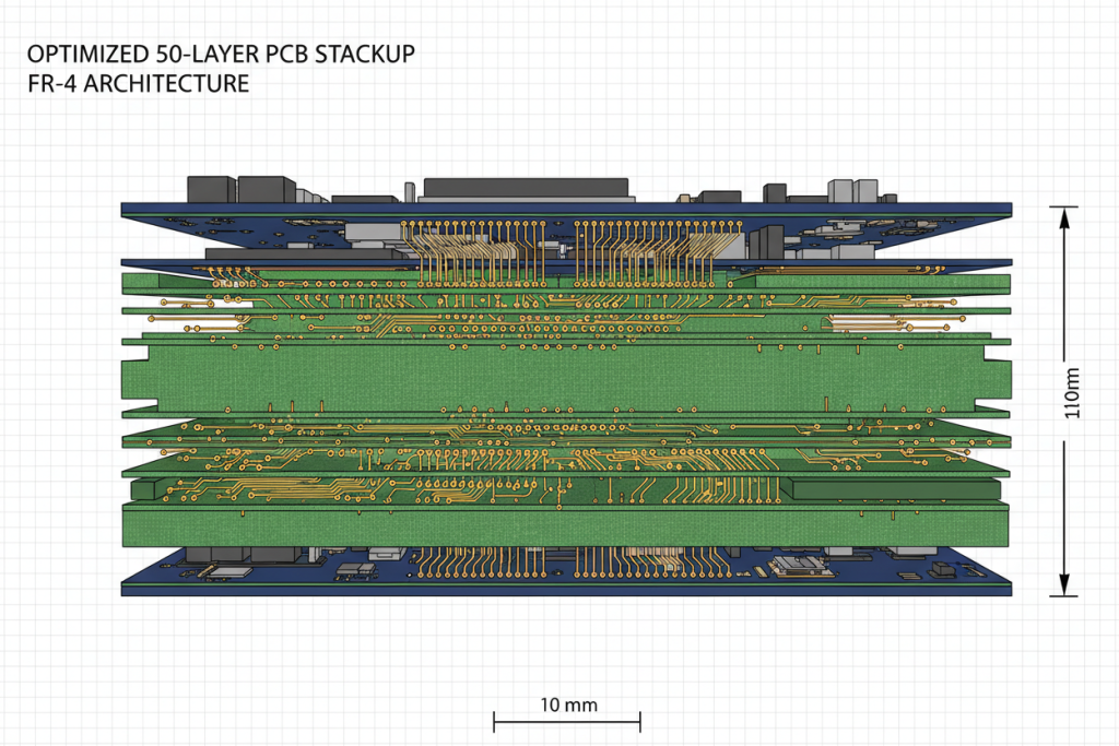
Figure 1: Cross-sectional view of optimized 50-layer FR-4 PCB stackup architecture
Stackup Architecture: Foundation of Signal Integrity
Symmetrical Layer Pairing Principles
For 50-layer FR-4 PCB design, symmetrical construction is non-negotiable. Asymmetrical stackups create bow and twist exceeding 0.75%—unacceptable for high-density connectors.
Recommended 50-Layer Stackup Configuration:
| Layer Group | Function | Material | Thickness (μm) |
|---|---|---|---|
| L1-L2 | Top signal + GND | FR-4 High Tg | 200 |
| L3-L8 | High-speed routing | Low-Dk FR-4 | 800 |
| L9-L16 | Power distribution | FR-4 + 2oz Cu | 1200 |
| L17-L34 | Core signal layers | Standard FR-4 | 2400 |
| L35-L42 | Secondary power | FR-4 + 1oz Cu | 1200 |
| L43-L48 | High-speed return | Low-Dk FR-4 | 800 |
| L49-L50 | Bottom GND + signal | FR-4 High Tg | 200 |
Critical stackup rules:
- Maintain ±5% symmetry around the centerline (between L25-L26)
- Separate high-speed layers by at least 400μm to minimize crosstalk
- Use low-Dk materials (εr < 3.8) for layers above 10 GHz operation
Material Selection for 50-Layer Boards
Not all FR-4 is created equal. For 50-layer applications, High Tg (glass transition temperature) materials are mandatory:
- Standard FR-4: Tg 130-140°C — insufficient for lead-free assembly
- High Tg FR-4: Tg 170-180°C — minimum for 50-layer reliability
- Very High Tg: Tg 200°C+ — required for aerospace applications
Design Note: When selecting materials for Special PCBs, verify the Z-axis expansion coefficient. Values below 3.0% (50-260°C) prevent via barrel cracking during thermal cycling.
Impedance Control and Routing Strategies
Single-Ended vs. Differential Impedance Targets
High-speed 50-layer designs require precise impedance control across all routing layers. The following table presents standard target values:
| Signal Type | Target Impedance | Tolerance | Layer Priority |
|---|---|---|---|
| DDR4 DQ/DQS | 40Ω single-ended | ±10% | L3, L6, L45, L48 |
| PCIe Gen5 | 85Ω differential | ±5% | L4, L5, L46, L47 |
| 100G Ethernet | 100Ω differential | ±5% | L3-L8, L43-L48 |
| RF Microwave | 50Ω single-ended | ±3% | L2, L49 (GND-adjacent) |
Routing Methodology for 50-Layer Designs
Step 1: Layer Assignment Strategy
Assign high-speed signals to layers closest to their reference planes. For 50-layer boards, this means:
- Critical signals: L3, L4, L47, L48 (adjacent to ground)
- Medium-speed: L5-L8, L43-L46
- Low-speed control: L17-L34 (inner layers)
Step 2: Via Transition Management
Minimize layer transitions for high-speed nets. Each via introduces 0.5-2 pF parasitic capacitance and inductance that degrades signal rise times.
Step 3: Length Matching Protocols
For 50-layer differential pairs:
- Intra-pair matching: ±5 mils (0.127 mm)
- Inter-pair matching: ±25 mils (0.635 mm) for DDR interfaces
- Use serpentine routing only on layers with consistent dielectric constants
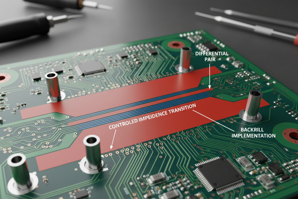
Figure 2: Optimized differential pair routing showing controlled impedance transitions and backdrill implementation
Via Optimization for High-Layer Count Designs
The Via Stub Problem
In 50-layer FR-4 PCBs, through-hole vias create significant stub effects. A via traversing all 50 layers presents a stub length of approximately 2.5 mm—catastrophic for signals above 3 GHz.
Solution: Backdrilling (Controlled Depth Drilling)
Backdrilling removes unused via portions, eliminating stub resonance. Implementation guidelines:
| Parameter | Specification | Manufacturing Tolerance |
|---|---|---|
| Backdrill depth | Target layer + 0.2 mm | ±0.1 mm |
| Remaining stub | < 0.25 mm | Process dependent |
| Drill diameter | +0.15 mm over primary drill | ±0.05 mm |
| Layer registration | ±0.075 mm | Critical for 50 layers |
Via Type Selection Matrix
For optimal 50-layer design, use this hierarchy:
- Microvias (Layers 1-2, 49-50): Laser-drilled, 0.1 mm diameter, lowest parasitics
- Blind vias (L1-L8, L43-L50): Mechanical drill, connect outer to inner layers
- Buried vias (L9-L42): Internal layer connections, no surface access
- Through vias: Power, ground, and low-speed signals only
Critical Warning: Avoid through-hole vias for signals exceeding 5 GHz in 50-layer designs. Even with backdrilling, residual stubs create impedance discontinuities exceeding ±15%.
Power Integrity and Thermal Management
PDN Design for 50-Layer Architectures
Power distribution in 50-layer boards requires plane segmentation and decoupling strategies that differ fundamentally from lower layer counts.
Plane Configuration:
- L9-L12: Primary 3.3V distribution (2oz copper)
- L13-L16: Primary 1.8V/1.2V distribution (split planes)
- L35-L38: Secondary 3.3V (1oz copper, backup)
- L39-L42: Secondary 1.0V/0.9V (AI core voltages)
Decoupling Capacitor Placement:
- 100 nF capacitors: Every 50 mm across all power entry points
- 10 μF bulk capacitors: At each power plane transition
- 1 μF capacitors: Adjacent to all high-speed IC power pins
Thermal Via Arrays
With 50 layers, thermal management requires dedicated via structures:
| Thermal Requirement | Via Array Pattern | Via Diameter | Plating |
|---|---|---|---|
| < 5W dissipation | 3×3 grid, 1.0 mm pitch | 0.3 mm | 25 μm Cu |
| 5-15W dissipation | 5×5 grid, 0.8 mm pitch | 0.25 mm | 35 μm Cu |
| > 15W dissipation | 7×7 grid, 0.6 mm pitch | 0.2 mm | 50 μm Cu + filled |
Manufacturing Considerations and DFM
Design for Manufacturability (DFM) Checklist
50-layer boards push manufacturing capabilities to limits. Adherence to DFM principles prevents costly delays:
Layer Registration:
- Cumulative registration tolerance: ±0.125 mm across 50 layers
- Individual layer-to-layer: ±0.025 mm
- Use sequential lamination for >30 layers
Copper Thickness Distribution:
- Outer layers: 35-70 μm (1-2 oz) for component mounting
- Inner layers: 17.5-35 μm (0.5-1 oz) for fine-line routing
- Power planes: 70 μm+ (2 oz) for current capacity
Annular Ring Requirements:
- Minimum annular ring: 0.125 mm (5 mils) for vias
- Target: 0.175 mm for reliability in thermal cycling
Manufacturing Insight: When sourcing Custom service with 7-day rapid delivery, provide complete stackup documentation and impedance requirements upfront. 50-layer prototypes require 3-5 day additional process time compared to standard 8-layer boards.
Testing Protocols for 50-Layer Boards
| Test Type | Coverage | Purpose | Acceptance Criteria |
|---|---|---|---|
| Flying probe | 100% nets | Open/short detection | 0 defects |
| Impedance TDR | All controlled lines | Zo verification | ±10% of target |
| X-section analysis | Sample vias | Layer registration, plating | IPC Class 3 |
| Thermal cycling | Sample lots | Reliability validation | 500 cycles, -40°C to +125°C |
Industry Applications and Use Cases
Use Case 1: 5G Baseband Processing Unit
Application: 64T64R massive MIMO base station controller
Layer Count: 48 layers (FR-4 hybrid with Rogers 4350B)
Key Design Features:
- 28 GHz RF routing on outer layers with Rogers material
- Digital processing on inner FR-4 layers
- 50-layer equivalent stackup with mixed dielectrics
- Backdrilled vias for 25 Gbps SerDes channels
Results: Achieved -35 dB return loss at 28 GHz, meeting 3GPP specifications.
Use Case 2: Satellite Communication Payload
Application: Geostationary satellite data router
Layer Count: 50 layers (All High Tg FR-4)
Key Design Features:
- Redundant power planes (L9-L16 primary, L35-L42 backup)
- Triple-redundant high-speed routing for fault tolerance
- Thermal via arrays dissipating 45W from FPGA clusters
- 15-year operational life requirement (space-grade)
Results: Passed 1000-cycle thermal vacuum testing with <0.1 dB insertion loss variation.
Use Case 3: AI Training Accelerator
Application: Data center GPU interconnect board
Layer Count: 46 layers (Very High Tg FR-4)
Key Design Features:
- 400 Gbps PAM4 signaling across 32 channels
- 1.0V/800A power delivery with 32-layer PDN
- Liquid cooling integration through thermal vias
- 0.5 mm pitch BGA breakout on 8 layers
Results: BER < 1×10⁻¹² at 400 Gbps, meeting IEEE 802.3bs standards.
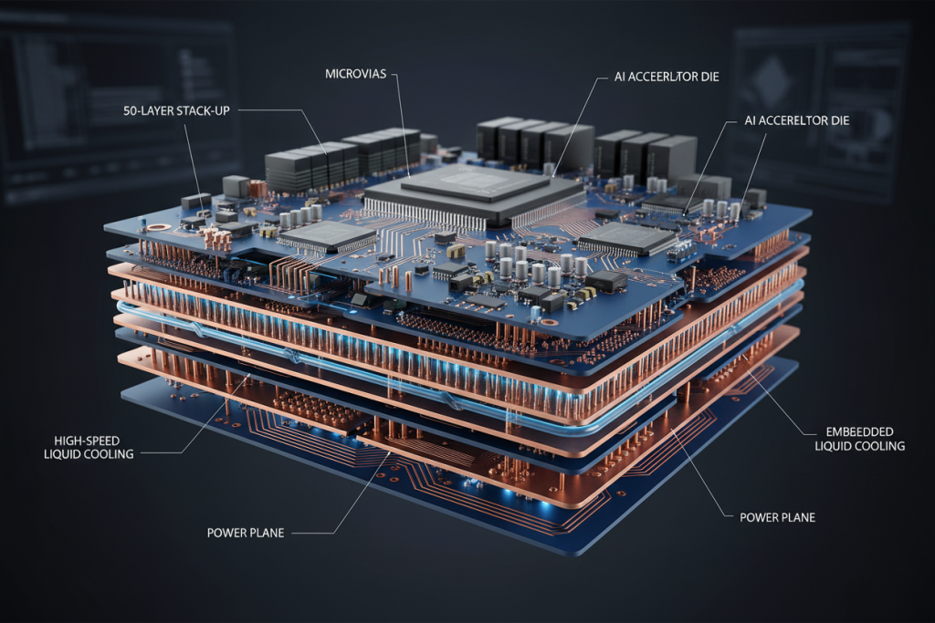
Figure 3: 50-layer PCB implementation in data center AI accelerator application
Frequently Asked Questions
What is the maximum thickness for 50-layer FR-4 PCBs?
50-layer FR-4 PCBs can achieve thicknesses from 3.0 mm to 20 mm depending on copper weights and prepreg selection. Standard designs typically range 4.0-8.0 mm. Thicknesses above 12 mm require sequential lamination processes and extended manufacturing cycles. For applications requiring Special PCBs with extreme thickness, consult manufacturers regarding drill aspect ratio capabilities (typically max 12:1 for mechanical drills).
How do you control impedance across 50 layers with varying dielectric heights?
Impedance control in 50-layer designs requires layer-specific trace width calculations. Use field solver software (HyperLynx, SI8000) to model each layer pair individually. Maintain consistent dielectric materials within high-speed layer groups. Implement ±10% impedance tolerance for single-ended, ±5% for differential pairs. Always include coupon structures for TDR verification during manufacturing.
What are the cost implications of 50-layer vs. 30-layer designs?
Cost scales non-linearly with layer count. 50-layer prototypes typically cost 2.5-3.5× equivalent 30-layer designs due to:
- Sequential lamination cycles (3-4 press cycles vs. 2)
- Extended drill times (50:1 aspect ratio management)
- Yield reduction (15-20% lower than 30-layer)
- Testing complexity (impedance verification on 40+ layers)
However, for high-density applications, 50-layer designs often eliminate the need for multiple PCBs and connectors, reducing total system cost by 15-25%.
Can 50-layer FR-4 PCBs support 112 Gbps PAM4 signaling?
Yes, with specific constraints. 112 Gbps PAM4 (56 GHz Nyquist) requires:
- Low-Dk FR-4 variants (εr < 3.5) for high-speed layers
- Maximum 12 mm trace lengths on standard FR-4
- Backdrilled vias with <0.15 mm residual stubs
- Insertion loss budget: -6 dB at 28 GHz (Nyquist)
For longer channels, hybrid constructions with Rogers 3000-series materials on outer layers are recommended.
What is the typical lead time for 50-layer PCB prototypes?
Standard lead times for 50-layer prototypes range 15-25 working days, compared to 5-8 days for 8-layer boards. Factors affecting delivery:
- Sequential lamination requirements (+5-7 days)
- Impedance testing and verification (+2-3 days)
- Layer registration qualification (+2 days)
For urgent projects, Custom service with 7-day rapid delivery options may be available for qualified designs with simplified stackups.
Conclusion and Next Steps
50-layer FR-4 PCB design represents the pinnacle of multilayer circuit board engineering, enabling next-generation applications in 5G, aerospace, and artificial intelligence. Success demands mastery of stackup symmetry, impedance control, via optimization, and thermal management—disciplines that separate functional prototypes from production-ready platforms.
Key takeaways from this guide:
- Symmetrical stackup design prevents warping and ensures manufacturability
- Backdrilling is essential for signal integrity above 5 GHz
- Power distribution requires dedicated plane strategies across 50 layers
- Material selection (High Tg, Low-Dk) directly impacts performance and reliability
As data rates continue escalating toward 224 Gbps and beyond, the principles outlined here provide the foundation for reliable high-layer count designs. The complexity is substantial, but with proper methodology, 50-layer FR-4 PCBs deliver unmatched density and performance.
Ready to transform your high-speed design concepts into reliable 50-layer implementations? Contact our engineering team today for stackup optimization support and manufacturing feasibility analysis.