6 Layer HDI PCB Assembly: Benefits for Compact Medical Devices
Medical device manufacturers face increasing pressure to deliver smaller, more powerful diagnostic and therapeutic equipment while maintaining the highest reliability standards. Six-layer HDI (High-Density Interconnect) PCB assembly has emerged as a critical enabling technology for compact medical devices, offering the density, performance, and biocompatibility required for modern healthcare applications.
This guide explains how 6-layer HDI PCB design and assembly addresses the unique challenges of medical electronics, from regulatory compliance to signal integrity in miniaturized form factors.
Table of Contents
- Why 6-layer HDI PCB matters for medical device miniaturization
- Critical design parameters for medical-grade 6-layer HDI assemblies
- Stackup design considerations for medical applications
- Assembly process requirements and quality standards
- Regulatory compliance and material selection
- Design trade-offs: cost vs performance vs reliability
- FAQ
- Conclusion and next steps
1. Why 6-layer HDI PCB matters for medical device miniaturization
Medical devices increasingly demand compact form factors without compromising functionality. Wearable glucose monitors, implantable cardiac devices, portable ultrasound systems, and handheld diagnostic tools all require high component density while maintaining signal integrity and electromagnetic compatibility.
Six-layer HDI PCB construction provides optimal balance between routing density and manufacturing feasibility for medical applications. Unlike traditional 4-layer boards that struggle with high-speed signal routing in constrained spaces, 6-layer HDI designs offer dedicated power and ground planes that improve noise immunity—critical when processing low-amplitude biosignals.
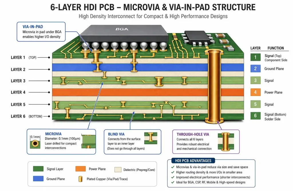
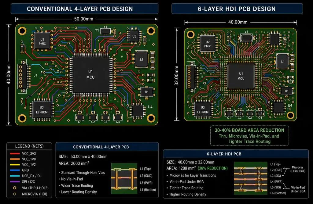
The HDI technology enables microvias (typically 0.1mm to 0.15mm diameter) and finer trace geometries (3mil/3mil or tighter), allowing component placement on both sides with via-in-pad configurations. This reduces board area by 30-40% compared to conventional PCB designs while improving electrical performance through shorter signal paths.
For medical devices operating in or near the human body, thermal management becomes critical. The additional internal layers in a 6-layer stackup facilitate better heat dissipation through strategically placed thermal vias and copper planes, preventing localized heating that could damage sensitive biological tissue or compromise electronic components.
2. Critical design parameters for medical-grade 6-layer HDI assemblies
Medical device PCB assemblies must meet IPC-6012 Class 3 requirements, which mandate tighter tolerances and more rigorous inspection than consumer electronics. Understanding these parameters during the design phase prevents costly respins and regulatory delays.
Trace width and spacing requirements
For 6-layer HDI medical PCBs, trace geometries depend on the current carrying requirements and signal integrity constraints. Minimum trace width should consider both manufacturing capability and current capacity with appropriate temperature rise margins.
| Parameter | IPC Class 2 | IPC Class 3 | Medical HDI Typical |
|---|---|---|---|
| Minimum trace width | 4 mil (0.1mm) | 4 mil (0.1mm) | 3-4 mil (0.075-0.1mm) |
| Minimum trace spacing | 4 mil (0.1mm) | 4 mil (0.1mm) | 3-4 mil (0.075-0.1mm) |
| Minimum annular ring | 2 mil (0.05mm) | 4 mil (0.1mm) | 3-4 mil (0.075-0.1mm) |
| Via diameter (mechanical) | 8 mil (0.2mm) | 8 mil (0.2mm) | 8-12 mil (0.2-0.3mm) |
| Microvia diameter | 4-6 mil (0.1-0.15mm) | 4-6 mil (0.1-0.15mm) | 4-6 mil (0.1-0.15mm) |
| Microvia aspect ratio | 1:1 preferred | 1:1 preferred | 1:1 (safer for reliability) |
For high-speed digital interfaces common in medical imaging devices (USB 3.0, HDMI, or proprietary protocols), differential pair routing requires matched impedance, typically 90Ω or 100Ω depending on the standard. Trace width calculation must account for the dielectric constant (Dk) of your prepreg material, typically FR4 with Dk around 4.2-4.5 at 1GHz.
Analog front-end circuits processing ECG, EEG, or biosensor signals demand careful ground plane management. A continuous ground plane on Layer 2 (just below the top signal layer) provides low-impedance return paths, reducing common-mode noise that could corrupt microvolt-level physiological signals.
Via design and placement rules
HDI PCBs use three types of vias: through-hole vias connecting all layers, blind vias connecting outer layers to inner layers, and buried vias connecting only internal layers. For medical 6-layer designs, microvia stacking is generally limited to 1+N+1 configuration (one microvia layer on top, N through-hole layers, one microvia layer on bottom) to balance density with reliability.
Via-in-pad design, where vias are placed directly under component pads, maximizes routing density but requires via plugging and planarization to ensure reliable solder joint formation. Medical devices using BGA components with fine pitch (0.5mm or tighter) often require this approach, but the via plug material must be compatible with lead-free reflow profiles.
3. Stackup design considerations for medical applications
The layer stackup defines signal integrity performance, EMI characteristics, and manufacturing yield. For 6-layer HDI medical PCBs, a well-designed stackup balances high-speed digital signals, sensitive analog circuits, and power distribution.
Recommended stackup configurations
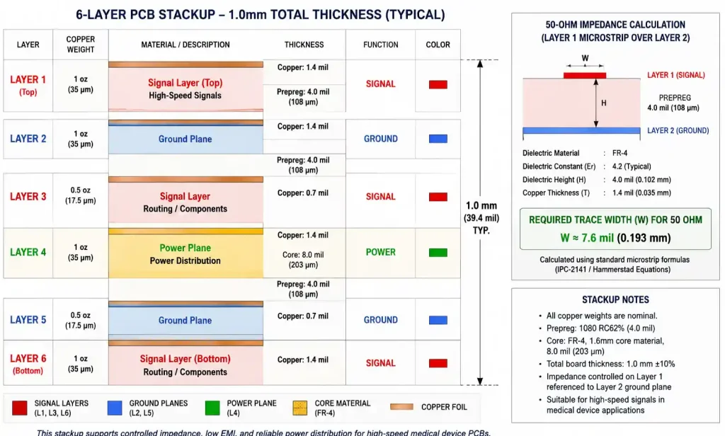
A typical 6-layer HDI stackup for medical devices prioritizes signal integrity and EMI control:
| Layer | Type | Copper Weight | Function | Dielectric Thickness |
|---|---|---|---|---|
| Layer 1 | Signal | 1 oz (35μm) | High-speed digital, RF (if applicable) | — |
| Layer 2 | Ground | 1 oz (35μm) | Continuous reference plane | 4 mil (0.1mm) prepreg |
| Layer 3 | Signal | 0.5 oz (17μm) | Internal routing, sensitive analog | 8 mil (0.2mm) core |
| Layer 4 | Power | 0.5 oz (17μm) | Split power planes (e.g., 3.3V, 5V, 12V) | 8 mil (0.2mm) core |
| Layer 5 | Ground | 1 oz (35μm) | Return path for bottom signals | 4 mil (0.1mm) prepreg |
| Layer 6 | Signal | 1 oz (35μm) | Component placement, power routing | — |
This asymmetric stackup places critical analog signals on Layer 3, sandwiched between two ground planes (Layers 2 and 4 acting as AC ground through decoupling capacitors), providing excellent shielding from digital switching noise on the outer layers.
For portable medical devices with battery power, the power plane on Layer 4 can be split into isolated voltage domains with careful stitching capacitor placement at domain boundaries to prevent return current discontinuities. Never route high-speed signals across split planes—this creates unpredictable return paths and EMI issues.
Total board thickness for a 6-layer HDI medical PCB typically ranges from 0.8mm to 1.2mm, depending on component height constraints and mechanical flexibility requirements. Wearable devices may push toward the thinner end while benchtop diagnostic equipment can use standard 1.0mm thickness.
Material selection and dielectric properties
FR4 remains the most common substrate for medical PCBs due to cost-effectiveness and well-understood material properties. However, medical applications often require high-Tg FR4 (glass transition temperature ≥170°C) to withstand multiple reflow cycles during assembly and potential sterilization processes.
For RF medical devices (wireless vital sign monitors, implantable telemetry), low-loss materials like Rogers RO4350B or Isola I-Tera MT40 may be used selectively on outer layers, laminated to an FR4 core to control cost while maintaining RF performance. The dielectric loss tangent (Df) becomes significant above 1GHz—standard FR4 has Df around 0.02, while Rogers materials achieve 0.004 or lower.
UL recognition is mandatory for medical device materials. Verify that your PCB fabricator sources materials with appropriate UL 94 V-0 flame ratings and UL file numbers documented in your design history file for FDA submission.
4. Assembly process requirements and quality standards
Medical device PCB assembly faces more stringent process controls than consumer electronics. IPC-A-610 Class 3 workmanship standards apply to medical applications, requiring zero cosmetic defects that could propagate into functional failures over the device’s operational lifetime.
Component placement and soldering considerations
BGA and QFN packages dominate modern medical electronics due to their compact footprint and good thermal performance. For 6-layer HDI assemblies, BGA packages with 0.5mm or 0.4mm pitch require precise placement (±0.05mm or better) and well-controlled reflow profiles to prevent opens or bridging.
Lead-free solder (SAC305: 96.5% Sn, 3% Ag, 0.5% Cu) is standard for medical devices to comply with RoHS directives in most markets. The higher melting point of lead-free solder (217-220°C vs 183°C for Sn-Pb eutectic) necessitates careful PCB material selection to avoid delamination during reflow.
Nitrogen reflow atmosphere reduces oxidation and improves solder joint reliability, particularly important for medical devices expected to function reliably for 5-10 years or more. While N2 reflow adds cost, the improvement in joint quality justifies the investment for Class 3 assemblies.
Inspection and testing protocols
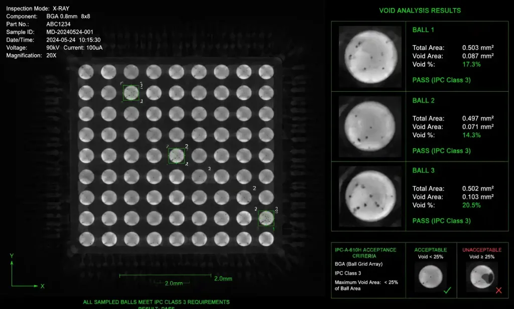
X-ray inspection is mandatory for all BGA and hidden solder joints on medical PCBs. The inspection must verify voiding percentage (typically <25% for Class 3), proper solder wetting, and absence of bridging. For assemblies with via-in-pad designs, X-ray confirms that via plugging hasn’t created voids under component pads.
| Test Method | Purpose | Acceptance Criteria (Class 3) |
|---|---|---|
| AOI (Automated Optical Inspection) | Surface mount placement, polarity, presence/absence | 100% component coverage, zero false accepts |
| X-ray inspection | BGA void analysis, hidden joints | <25% void area per ball, no bridging |
| Flying probe test | Electrical continuity, shorts | 100% net coverage, no opens/shorts |
| Functional test | System-level operation | Per device specification |
| Boundary scan (if designed in) | Digital circuit connectivity | 100% coverage of JTAG-enabled devices |
Beyond standard electrical testing, medical devices often require ESS (Environmental Stress Screening) including thermal cycling and vibration testing on a sample basis to detect latent defects before field deployment. For implantable devices, hermeticity testing and accelerated aging under simulated body fluid conditions validate long-term reliability.
5. Regulatory compliance and material selection
Medical device PCBAs must comply with ISO 13485 quality management systems and region-specific regulations: FDA 510(k) or PMA in the United States, CE marking under MDR in Europe, and NMPA approval in China.
Biocompatibility and material safety
For devices contacting patient skin or implanted in the body, PCB materials must undergo biocompatibility testing per ISO 10993 series standards. This typically includes cytotoxicity, sensitization, and irritation testing. Most FR4 laminate materials pass these tests, but conformal coatings and solder mask materials require specific qualification.
Parylene coating provides excellent biocompatible barrier protection for implantable electronics, offering pinhole-free coverage even on complex 3D geometries. The coating process occurs at room temperature under vacuum, eliminating thermal stress on assembled components.
Traceability and documentation requirements
Every medical PCB assembly requires complete traceability from raw materials through final test. This includes:
- Material certifications (UL file numbers, RoHS compliance, conflict minerals declarations)
- PCB fabrication lot traceability with coupon test results
- Component lot codes and moisture sensitivity level (MSL) handling records
- Assembly process parameters (reflow profile data, solder paste batch numbers)
- Inspection and test records with images for each serial number
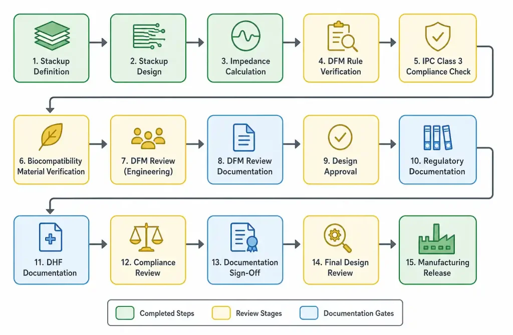
The design history file (DHF) must document all design decisions, including rationale for stackup selection, material choices, and design rule deviations. This documentation becomes critical during regulatory audits and post-market surveillance investigations.
6. Design trade-offs: cost vs performance vs reliability
Medical device development involves balancing competing requirements: miniaturization drives complexity and cost, while reliability demands conservative design margins.
Prototype vs production considerations
Initial prototypes for medical devices often use 6-layer HDI to validate the compact form factor, but production may revert to conventional PCB construction if cost pressure outweighs density benefits. A 6-layer HDI PCB typically costs 2-3× more than a comparable 6-layer conventional board due to laser drilling, sequential lamination, and tighter process controls.
However, the system-level cost equation includes enclosure size, cable length, and EMI shielding requirements. A slightly more expensive HDI PCB that eliminates external shielding cans and reduces enclosure volume can deliver lower total system cost, particularly for high-volume wearable devices.
| Design Approach | Board Cost Multiplier | Typical Use Case | Manufacturing Lead Time |
|---|---|---|---|
| 4-layer conventional | 1.0× (baseline) | Low-complexity patient monitors, simple diagnostic tools | 5-7 days (prototype) |
| 6-layer conventional | 1.3-1.5× | Multi-function vital signs monitors, portable ultrasound | 7-10 days (prototype) |
| 6-layer HDI (1+4+1) | 2.5-3.0× | Wearable CGM, implantable devices, compact imaging systems | 10-15 days (prototype) |
| 8-layer HDI (2+4+2) | 3.5-4.5× | High-resolution imaging, complex RF telemetry, AI processors | 15-20 days (prototype) |
Production lead times decrease as volume increases, but medical devices typically operate at lower volumes than consumer products, so prototype-level pricing often persists into production for specialized diagnostic equipment.
Design margin philosophy for medical applications
Medical device reliability targets often specify MTBF (Mean Time Between Failures) exceeding 100,000 hours under operating conditions. Achieving this requires conservative design margins beyond what semiconductor datasheets recommend.
For power supply circuits, operate switching regulators at 60-70% of maximum rated current rather than the 80-90% common in consumer devices. This reduces thermal stress and extends capacitor lifetime, critical since electrolytic capacitors are often the first component to fail in medical electronics.
Similarly, route high-speed signals with impedance margins. If your ADC interface specifies 50Ω ±10%, design for 50Ω ±5% to account for manufacturing variations in dielectric thickness and trace etching. The controlled impedance option from your PCB fabricator should specify ±10% or tighter tolerance, with TDR (Time Domain Reflectometry) testing documentation for each production lot.
7. FAQ
What is the minimum trace width I can reliably manufacture on a 6-layer HDI medical PCB?
Most PCB manufacturers targeting medical applications can reliably produce 3mil (0.075mm) traces with 3mil spacing for 6-layer HDI boards. However, for Class 3 assemblies requiring tighter process control, staying at 4mil/4mil (0.1mm/0.1mm) improves yield and long-term reliability. The choice depends on routing density requirements—BGA escape routing with 0.5mm pitch typically needs 3mil capabilities, while 0.65mm pitch can be routed with 4mil rules.
How does HDI construction improve signal integrity for medical biosensor applications?
HDI enables shorter trace lengths through higher routing density and via-in-pad designs, reducing parasitic inductance and capacitance in sensitive analog signal paths. For ECG front-ends processing sub-millivolt signals, every millimeter of trace length adds noise pickup area. HDI microvias also have lower parasitic inductance than through-hole vias (approximately 0.1nH per via versus 1-2nH), improving power delivery network performance for high-speed ADCs.
What surface finish is recommended for medical device PCBs?
ENIG (Electroless Nickel Immersion Gold) is the most common surface finish for medical PCBs due to its flat surface (excellent for fine-pitch components), good solderability, and shelf life exceeding 12 months. The nickel layer (typically 3-6μm) provides a wear-resistant contact surface for edge connectors or test points. For cost-sensitive applications, Immersion Silver offers good performance, but requires tighter storage controls. Avoid HASL (Hot Air Solder Leveling) for fine-pitch components due to surface planarity issues.
Can I mix microvia and conventional via structures on the same 6-layer HDI board?
Yes, this is standard practice. Microvias (0.1-0.15mm diameter) are used in high-density areas for BGA escape routing and fine-pitch component connections, while conventional mechanical vias (0.2-0.3mm diameter) handle power distribution and lower-density signal routing. Using conventional vias where possible reduces manufacturing cost since laser drilling is more expensive than mechanical drilling. Ensure your CAM engineer receives clear fabrication notes identifying which vias are microvias versus standard vias.
How do I ensure electromagnetic compatibility (EMC) for a compact medical device using 6-layer HDI PCB?
EMC performance starts with proper stackup design: place continuous ground planes adjacent to signal layers, minimize split planes, and use grounded guard traces around sensitive analog circuits. For radiated emissions, ensure high-speed digital signals (clocks above 10MHz) route on internal layers rather than outer layers. Decoupling capacitors should be placed close to power pins with minimal via inductance—this is where HDI via-in-pad shines. Pre-compliance testing with near-field probes during development identifies problem areas before formal EMC chamber testing.
What DFM considerations are unique to medical-grade 6-layer HDI assemblies?
Beyond standard DFM rules, medical Class 3 assemblies require increased annular ring (minimum 4 mils for through-hole vias), no acid traps in copper patterns (sharp internal angles that can trap etchant and cause delayed failures), and increased clearance to board edges (minimum 0.5mm for mechanical vias, 1.0mm preferred). Panelization design must include test coupons for impedance verification, and X-ray targets for AOI calibration. If using via-in-pad, specify whether the fabricator or assembler performs plugging—this affects design rules for pad size and paste mask openings.
8. Conclusion and next steps
Six-layer HDI PCB assembly enables the next generation of compact, high-performance medical devices while meeting stringent regulatory and reliability requirements. The technology delivers measurable benefits in board area reduction, signal integrity, and thermal management compared to conventional PCB constructions.
For medical device engineers starting a new design, prioritize these decisions early: confirm your PCB fabricator has Class 3 capability and medical device experience, select materials with appropriate UL recognition and biocompatibility testing if needed, and design your stackup to separate sensitive analog circuits from digital switching noise.
Before submitting Gerber files for fabrication, conduct a DFM review focused on via aspect ratios, trace width/spacing margins, and annular ring adequacy for Class 3 requirements. Many PCB manufacturers offer free DFM analysis for medical projects—use this service to catch issues before committing to tooling.
If you’re evaluating whether 6-layer HDI justifies the cost premium for your application, consider the system-level equation: smaller boards enable smaller enclosures, shorter cables reduce EMI and component cost, and improved signal integrity may eliminate analog filter stages or allow lower-cost ADCs. The PCB cost difference often disappears at the system level.
Ready to move forward with your medical device PCB design? Submit your preliminary stackup and design constraints for a free feasibility review and manufacturing cost estimate. Our CAM engineering team can provide specific design rules tailored to your target manufacturing capability and volume requirements.