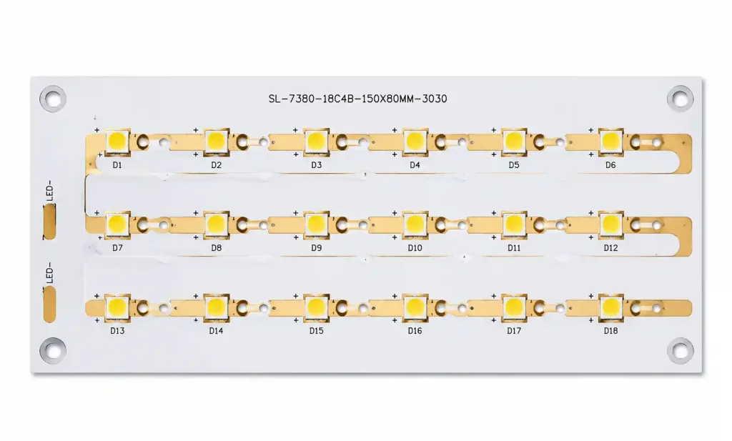
Street Light and High-Bay LED Fixtures: Aluminum PCB Design Requirements
When designing LED lighting systems for street lights and high-bay industrial fixtures, thermal management becomes the critical design constraint. Unlike consumer electronics where signal integrity or miniaturization dominate, outdoor and industrial LED applications demand PCBs that can dissipate 50-150W of heat while surviving temperature swings from -40°C to +85°C, moisture exposure, and decades of continuous operation.
This guide covers the aluminum PCB design parameters, material selection criteria, thermal interface requirements, and DFM considerations specific to high-power LED street lighting and high-bay fixtures. Whether you’re designing a 100W street light module or a 200W warehouse high-bay array, understanding how copper thickness, dielectric thermal conductivity, and solder mask design affect both lumens-per-watt efficiency and long-term reliability will directly impact your product’s field performance and warranty costs.
Table of Contents
- Why Aluminum PCBs Are Essential for High-Power LED Lighting
- Critical Design Parameters for Street Light and High-Bay LED PCBs
- Aluminum Base Material Selection and Thermal Performance
- Copper Layer Design: Thickness, Trace Width, and Current Carrying Capacity
- Thermal Interface and Dielectric Layer Requirements
- DFM Considerations for LED Aluminum PCB Manufacturing
- FAQ
- Conclusion and Design Verification Steps
1. Why Aluminum PCBs Are Essential for High-Power LED Lighting
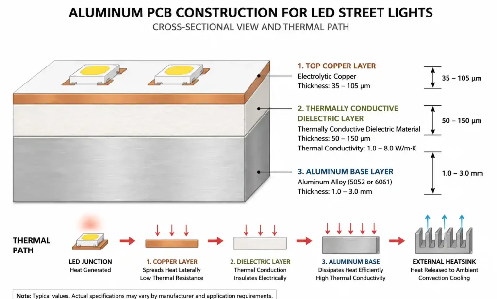
Street lights and high-bay fixtures operate in the 50-250W power range, with LED junction temperatures that must stay below 125°C to maintain lumen output and prevent accelerated degradation. Standard FR4 PCBs have thermal conductivity around 0.3-0.4 W/m·K, which creates hotspots and shortens LED lifespan. Aluminum-based PCBs, with thermal conductivity ranging from 1.0 to 8.0 W/m·K depending on dielectric material choice, provide a direct thermal path from LED die to heatsink.
For outdoor street lighting applications, additional environmental stresses include:
- Thermal cycling from daytime ambient heat to nighttime cold, causing CTE mismatch stress at solder joints
- High humidity and condensation exposure requiring conformal coating compatibility
- Vibration from wind load and mounting structure resonance
- Long operational life requirements (typically 50,000-100,000 hours L70 specification)
High-bay industrial fixtures face similar thermal loads but with added constraints from dusty or corrosive environments and the need for dimming driver compatibility. The aluminum PCB must not only dissipate heat efficiently but also provide a robust mounting interface, accommodate high-current LED strings, and survive wave soldering or reflow assembly without warping.
2. Critical Design Parameters for Street Light and High-Bay LED PCBs
The following table summarizes the key design parameters that differentiate LED aluminum PCBs from standard single-layer aluminum boards used in lower-power applications.
| Parameter | Street Light (50-150W) | High-Bay (100-250W) | Design Rationale |
|---|---|---|---|
| Copper thickness | 2 oz (70 μm) | 3 oz (105 μm) | Higher current density requires thicker copper to minimize resistive losses and heat generation in traces |
| Dielectric thermal conductivity | 2.0-3.0 W/m·K | 3.0-5.0 W/m·K | High-bay fixtures with denser LED arrays need faster heat transfer to prevent junction temperature runaway |
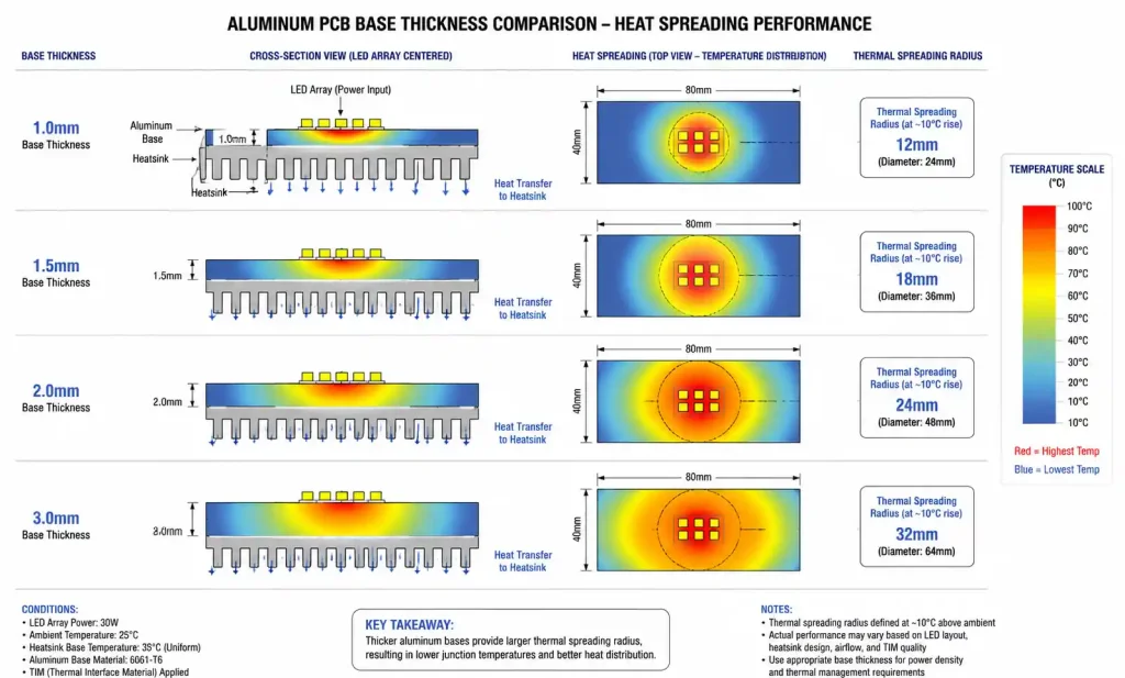
| Aluminum base thickness | 1.5-2.0 mm | 2.0-3.0 mm | Thicker base improves mechanical rigidity and provides larger thermal mass for transient load handling |
| Dielectric breakdown voltage | ≥3000 VAC | ≥3500 VAC | High-voltage LED strings (up to 200V DC) require sufficient insulation margin for safety certification |
| Solder mask | White reflective | White or black | White solder mask maximizes light reflection efficiency; black used for aesthetic or glare control |
| Surface finish | HASL or ENIG | ENIG preferred | ENIG provides better solder joint reliability under thermal cycling and eliminates lead-free soldering issues |
| LED pad size | 3-5 mm² per contact | 5-8 mm² per contact | Larger pads improve thermal coupling and accommodate high-power LED packages (3535, 5050, or 7070 footprints) |
For street light applications, design priority is balancing cost with adequate thermal performance and long-term reliability. High-bay fixtures, especially those operating 24/7 in warehouses or factories, justify the higher material cost of premium dielectric layers (3-5 W/m·K) to achieve lower junction temperatures and longer maintenance intervals.
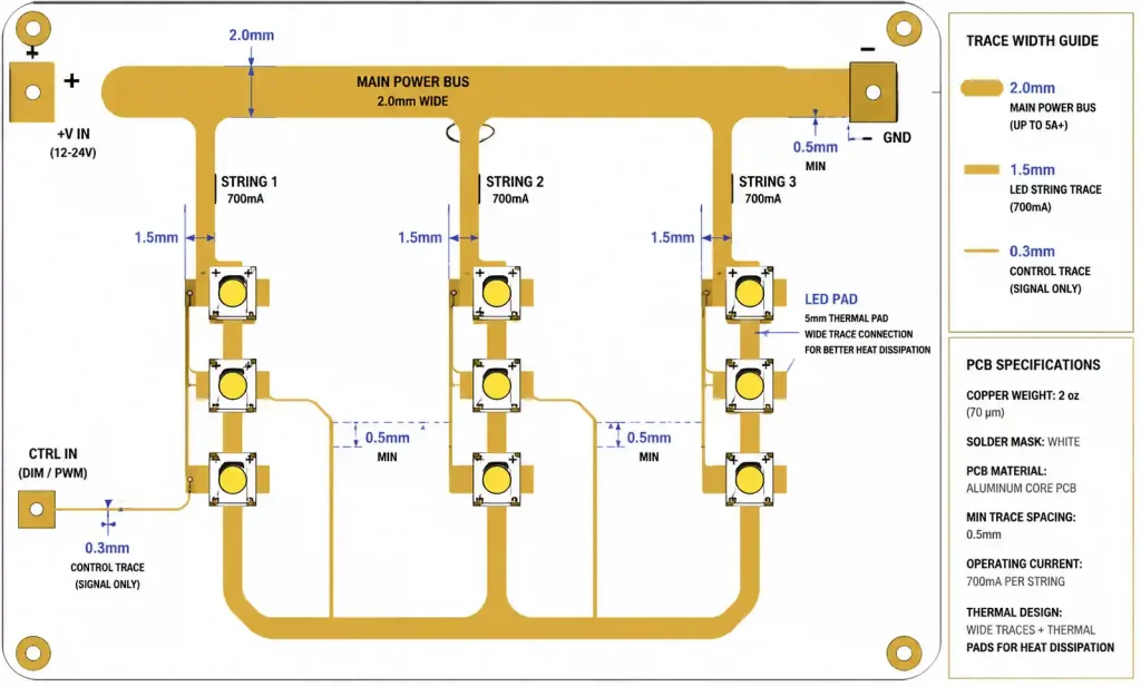
When routing LED strings in series, the trace width must accommodate the forward current (typically 350-1050 mA per string) while keeping copper temperature rise below 10°C above ambient. For 700 mA operation on 2 oz copper, minimum trace width should be 1.5 mm for continuous current paths; for 3 oz copper, 1.0 mm is acceptable. Always calculate trace width based on IPC-2152 current carrying capacity charts adjusted for aluminum PCB thermal dissipation.
3. Aluminum Base Material Selection and Thermal Performance
The aluminum base serves three functions: structural support, thermal spreading, and heat sink mounting interface. Most LED aluminum PCBs use 5052 or 6061 aluminum alloy, with 1.0-3.0 mm thickness depending on power level and mechanical requirements.
| Aluminum Alloy | Thermal Conductivity | Typical Thickness | Application |
|---|---|---|---|
| 5052-H32 | 138 W/m·K | 1.0-1.5 mm | Cost-optimized street lights, lower mechanical stress |
| 6061-T6 | 167 W/m·K | 1.5-2.0 mm | Standard choice for most LED applications, good machinability |
| 1100-H14 | 222 W/m·K | 2.0-3.0 mm | Maximum thermal performance for ultra-high-power arrays, higher cost |
Thicker aluminum bases (2.0-3.0 mm) provide better thermal spreading for clustered LED arrays, reducing the peak temperature at the center of the array. For street lights with linear LED arrangements, 1.5 mm thickness is usually sufficient. High-bay fixtures with dense 2D LED matrices benefit from 2.0-3.0 mm bases to spread heat laterally before transferring to the external heatsink.
The aluminum base must be flat within ±0.1 mm across the PCB area to ensure good thermal contact with the heatsink. Warpage during reflow soldering is a common manufacturing issue—specify a maximum reflow profile of 260°C peak temperature with a 60-90 second time above 217°C to prevent excessive aluminum expansion. Some manufacturers apply pre-baking at 120°C for 2 hours to reduce moisture-related warpage.
4. Copper Layer Design: Thickness, Trace Width, and Current Carrying Capacity
LED aluminum PCBs are typically single-layer designs with copper on top of the dielectric, eliminating the need for vias or multilayer stackups. Copper thickness directly affects both electrical performance (resistance and current handling) and thermal performance (heat spreading before transfer to dielectric).
Copper Thickness Selection
| Copper Weight | Thickness | Maximum Continuous Current (per mm width) | Best Application |
|---|---|---|---|
| 1 oz | 35 μm | 1.0 A | Low-power indicator LEDs, not recommended for street/high-bay |
| 2 oz | 70 μm | 2.0 A | Standard for 50-100W street lights, 350-700 mA LED strings |
| 3 oz | 105 μm | 3.0 A | High-power high-bay fixtures, 1000+ mA LED strings |
| 4 oz | 140 μm | 4.0 A | Extreme power applications, rarely needed for typical LED lighting |
For a 100W street light operating at 36V with 2.8A total current, using 2 oz copper with 2.0 mm wide power traces keeps copper temperature rise below 10°C. If the design uses parallel LED strings (e.g., 6 strings of 700 mA each), individual string traces can be narrower (1.5 mm) since each carries lower current.
Trace Width and Spacing
Minimum trace width should be calculated based on current density, not just manufacturing capability. While aluminum PCB manufacturers can etch 0.15 mm traces, LED power traces should follow these guidelines:
- Power traces (main supply): 2.0-3.0 mm width for 1-3A current
- LED string traces: 1.0-2.0 mm width for 350-1050 mA per string
- Driver control signals: 0.3-0.5 mm width (low current, can use minimum capability)
- Spacing between traces: minimum 0.5 mm for voltages <60V, 1.0 mm for >60V
Wider traces also improve thermal spreading from the LED pads. For high-power LEDs (3W+), the trace connecting to the thermal pad should be at least as wide as the pad itself to avoid creating a thermal bottleneck.
5. Thermal Interface and Dielectric Layer Requirements
The dielectric layer between copper and aluminum base is the critical thermal bottleneck in aluminum PCB design. This layer must provide electrical insulation (typically 3000-4000 VAC breakdown voltage) while transferring heat efficiently. Dielectric thickness ranges from 50-200 μm, with thinner layers offering better thermal conductivity but reduced breakdown voltage margin.
Dielectric Material Comparison
| Dielectric Type | Thermal Conductivity (W/m·K) | Thickness | Breakdown Voltage | Cost Level |
|---|---|---|---|---|
| Standard epoxy | 1.0-1.5 | 100-150 μm | 3000 VAC | Low |
| Ceramic-filled epoxy | 2.0-3.0 | 75-125 μm | 3500 VAC | Medium |
| High-performance polymer | 3.0-5.0 | 50-100 μm | 4000 VAC | High |
| Thermally conductive ceramic | 5.0-8.0 | 50-75 μm | 4500 VAC | Very high |
For street lights operating at 24-48V DC with moderate power density, a 2.0-3.0 W/m·K dielectric provides good balance between cost and thermal performance. High-bay fixtures running at higher voltages (100-200V LED strings) or with dense LED arrays should use 3.0-5.0 W/m·K materials to keep junction temperatures within spec.
The thermal resistance from LED junction to aluminum base can be calculated as:
R_th = (t_die + t_solder + t_copper + t_dielectric/k_dielectric) / A
Where:
- t_die = LED package thermal resistance (from datasheet)
- t_solder = solder joint thickness (~50 μm)
- t_copper = copper thickness (35-105 μm)
- t_dielectric = dielectric layer thickness (50-150 μm)
- k_dielectric = dielectric thermal conductivity (1.0-8.0 W/m·K)
- A = effective thermal spreading area
For a typical 3W LED with 10 mm² thermal pad, using 75 μm dielectric at 3.0 W/m·K, the dielectric layer contributes approximately 2.5°C/W to the total thermal resistance. Doubling the thermal conductivity to 6.0 W/m·K reduces this to 1.25°C/W—a significant improvement for high-power arrays.
Always verify that the dielectric breakdown voltage exceeds the maximum LED string voltage by at least 5x margin for safety certification. A 48V LED string should use a dielectric rated for at least 2400V, but 3000-3500V is standard industry practice.
6. DFM Considerations for LED Aluminum PCB Manufacturing
Aluminum PCBs have different manufacturing constraints compared to FR4 boards, and several DFM issues are specific to LED lighting applications.
Manufacturing Checklist for LED Aluminum PCBs
| Design Item | Requirement | Risk if Violated | Recommended Action |
|---|---|---|---|
| Copper-to-edge clearance | ≥3.0 mm | Copper delamination during routing, electrical short to aluminum base | Add keepout zone in layout, verify with DFM report |
| LED pad solder mask opening | Pad size + 0.2 mm | Poor solder wetting, solder ball formation | Use solder mask defined pads for LEDs <5mm², NSMD for >5mm² |
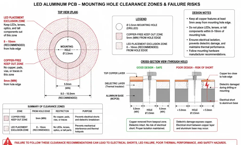
| Mounting hole to copper clearance | ≥5.0 mm | Electrical short if screw contacts copper | Add ground plane isolation around mounting holes |
| V-cut or routing clearance | ≥1.5 mm from edge to copper | Board breakage, copper damage during depaneling | Design panel with 1.5-2.0 mm border |
| Aluminum base flatness | ≤0.1 mm across board | Poor thermal contact with heatsink, uneven LED temperature | Specify flatness tolerance on fabrication drawing |
| Thermal pad via prohibition | No vias allowed | Not applicable to single-layer aluminum PCB | Design rule: disable via placement in thermal zones |
| White solder mask coverage | 100% coverage except pad openings | Reduced light reflection efficiency | Verify solder mask artwork includes all non-functional areas |
One common DFM error in LED designs is placing LEDs too close to the board edge. For street lights that mount directly to a heatsink with screws around the perimeter, maintain at least 8-10 mm from LED center to mounting hole center. This prevents thermal gradients from causing uneven light output across the array.
Another frequent issue is insufficient copper-to-aluminum base clearance around mounting holes. If the mounting screw or heatsink makes electrical contact with the copper layer through a damaged dielectric, it can create a ground fault or short circuit. Always specify a 5 mm copper-free zone around mounting holes and verify this in the Gerber files before fabrication.
Solder Mask Design for Reflectivity
White solder mask is standard for LED aluminum PCBs to maximize light extraction efficiency by reflecting stray photons back through the lens. The solder mask must be applied uniformly without voids or thin spots that could cause discoloration over time from LED heat exposure.
Key solder mask specifications:
- Color: white (reflectivity >85%) or matte black (for glare-sensitive applications)
- Thickness: 15-25 μm over copper
- Solder dam between pads: minimum 0.3 mm for wave soldering, 0.2 mm for reflow
- Opening tolerance: ±0.1 mm from pad edge
For high-bay fixtures where maintenance personnel look up at the light source, matte black solder mask reduces glare but sacrifices 5-10% optical efficiency. The trade-off depends on the fixture’s optical design and lens characteristics.
7. FAQ
What is the difference between aluminum PCB and MCPCB for LED applications?
MCPCB (Metal Core PCB) is a general term that includes aluminum-base, copper-base, and steel-base PCBs. For LED lighting, “aluminum PCB” and “aluminum MCPCB” are used interchangeably—both refer to the same single-layer copper-on-aluminum-base construction. Copper-base MCPCBs offer higher thermal conductivity (380 W/m·K vs 138-222 W/m·K) but cost 3-5x more and are only justified for extreme power densities above 50 W/in².
How do I calculate the required thermal conductivity for my LED array?
First, determine the total LED power dissipation (optical output + driver losses). Calculate the maximum allowable junction temperature based on LED datasheet (typically 125°C limit). Measure the ambient temperature inside your fixture (not room temperature—account for heatsink temperature rise). The required thermal resistance is R_th = (T_junction – T_ambient) / P_total. Then work backwards: given your dielectric thickness and copper thickness, solve for the required k_dielectric. Most street lights need 2-3 W/m·K; high-bay fixtures need 3-5 W/m·K.
Can I use aluminum PCB with wave soldering?
Yes, but with restrictions. The aluminum base acts as a large thermal mass that slows heating and cooling, making temperature profile control difficult. Pre-heat the board to 120-150°C before wave contact to reduce thermal shock. Reflow soldering is preferred for LED assembly because the oven profile can be tuned to the aluminum PCB’s thermal mass. If wave soldering is required, use HASL surface finish and avoid ENIG, which can suffer from brittle solder joints under rapid cooling.
What is the minimum copper-to-aluminum base clearance for electrical safety?
IPC-2221 requires minimum clearance based on voltage: for <50V, 0.13 mm is sufficient, but practical manufacturing tolerances and dielectric breakdown margin push this to 0.5-1.0 mm. For LED strings above 60V, use 1.5-2.0 mm clearance between copper and any area where the dielectric might be damaged (board edges, mounting holes, V-cut grooves). Always design for a 5x safety margin on dielectric breakdown voltage relative to operating voltage.
Should I use HASL or ENIG surface finish for outdoor LED street lights?
ENIG is preferred for street lights because it provides better solder joint reliability under thermal cycling (-40°C to +85°C daily swings) and eliminates the lead-free soldering issues associated with HASL. HASL can work for indoor high-bay fixtures with stable temperatures. ENIG costs 15-20% more but significantly reduces field failures from solder joint cracking after 5-10 years of operation. If cost is critical, OSP (Organic Solderability Preservative) is an alternative, but it has a shorter shelf life and requires careful handling during assembly.
How thick should the aluminum base be for a 150W high-bay LED fixture?
For 150W dissipated across a 150-200 cm² board area, use 2.0 mm aluminum base (6061-T6 alloy). Thinner bases (1.5 mm) may warp during reflow or exhibit poor flatness when bolted to the heatsink. Thicker bases (3.0 mm) provide better thermal spreading for dense LED clusters but add weight and cost. The optimal thickness depends on LED spacing: for distributed arrays, 1.5-2.0 mm is adequate; for high-density clusters (>10 LEDs in a 50 cm² area), use 2.5-3.0 mm to spread heat laterally before it reaches the dielectric layer.
What are common causes of LED aluminum PCB delamination?
Delamination between copper and dielectric or dielectric and aluminum base typically results from: (1) Excessive reflow temperature—keep peak temperature below 260°C and limit time above liquidus to <90 seconds. (2) Moisture absorption before soldering—bake boards at 120°C for 2-4 hours if stored in humid conditions. (3) CTE mismatch stress from thermal cycling—use dielectric materials with CTE matched to aluminum (23-24 ppm/°C). (4) Poor surface preparation during manufacturing—verify that the aluminum base is properly treated (anodized or chemically treated) for adhesion. Always request a cross-section analysis from your PCB manufacturer to verify layer adhesion quality before volume production.
8. Conclusion and Design Verification Steps
Aluminum PCB design for street lights and high-bay LED fixtures requires balancing thermal performance, electrical safety, optical efficiency, and manufacturing cost. The critical design decisions—copper thickness, dielectric thermal conductivity, aluminum base thickness—directly determine whether your fixture meets L70 lifetime targets and passes safety certification.
Before submitting your design for manufacturing:
- Thermal simulation: Use FEA tools (ANSYS, SolidWorks Thermal, or LED manufacturer’s tools) to verify that junction temperatures stay below 125°C under worst-case conditions (maximum ambient + maximum drive current + minimum heatsink performance).
- DFM review: Submit Gerber files to your aluminum PCB manufacturer for a free DFM check. Verify copper-to-edge clearance, mounting hole keepouts, solder mask coverage, and board flatness specifications.
- Material selection verification: Confirm that the dielectric thermal conductivity, breakdown voltage, and aluminum alloy match your thermal and electrical requirements. Request material certifications (UL recognition for dielectric, alloy specification for aluminum base).
- Prototype testing: Build 5-10 prototype boards and run accelerated thermal cycling tests (-40°C to +85°C, 500 cycles minimum) while monitoring LED forward voltage shift. A 5% Vf increase indicates junction temperature stress or solder joint degradation.
For additional design support, download our LED Aluminum PCB Design Checklist or submit your Gerber files for a free thermal and DFM review by our CAM engineering team. We can verify your trace width calculations, dielectric thermal resistance, and mounting hole clearances before you commit to volume production.