
Skip to content
Andwin Circuits
  • Home
  • ProductsExpand
    • HDI multilayer PCB
    • Rigid Flex PCB
    • Flex pcb
    • Special PCBExpand
      • High Frequency PCBExpand
        • Rogers RO4350B PCB
        • Rogers RO4003 pcb
        • Rogers RO3003 PCB
        • Rogers 5880 PCB
        • DICLAD 527 PCB
        • Taconic TLX series
        • Taconic TLX-8 RF PCB
        • Taconic TLX-9 RF PCB
      • High speed pcbExpand
        • Megtron 6 High Speed PCB
        • TU-872 SLK Sp High Speed
      • High TG PCBExpand
        • SHENGYI SH260 PCB
        • ISOLA 370HR PCB
        • ISOLA IS410 PCB
        • ISOLA IS420 PCB
      • Heavy copper PCB
      • Copper coin pcb
      • Copper inlay PCB
    • Metal Core PCBExpand
      • Copper core pcb
      • Aluminum PCB
      • 2 Layers Aluminum PCB
      • Direct thermal MCPCB
      • 2 Layers Direct Thermal
    • Ceramic PCBExpand
      • DPC ceramic PCB
      • DBC ceramic PCB
      • Thick film Ceramic PCB
      • Al2O3 Alumina PCB
      • AIN ALN ceramic PCB
      • IGBT Ceramic PCB
  • ServiceExpand
    • PCB Assembly
    • Quick turn PCB assembly
    • PCBA conformal coating
  • IndustryExpand
    • Telecommunication
    • IoT and Wireless
    • Industrial Control
    • Thermal management
    • Power and Energy
    • IC test board
    • Automative
    • Medical
  • CapabilityExpand
    • Rigid PCB
    • Rigid flex PCB
    • Metal core PCB
    • PCB Assembly
  • TechnologyExpand
    • Blogs
    • Via in pad
    • PCB E-test
    • PCB stack up
    • MCPCB panelization
    • Controlled impedance PCB
  • AboutExpand
    • About us
    • Certification
    • Factory Tour
  • Contact
Andwin Circuits
Home / 6 layer pcb manufacturing

6 layer pcb manufacturing

ByGrace July 9, 2024July 9, 2024

Analysis of the key steps and technical points of 6 layer PCB manufacturing The manufacturing process of 6-layer printed circuit boards (PCBs) is complex and delicate, involving multiple key steps and technical points. The manufacturing process of 6-layer PCB involves multiple key steps and technical points, from design, material selection, inner and outer layer pattern production, lamination, drilling, electroplating, surface treatment to final electrical testing and quality control, each step is crucial. Only by strictly controlling each link can we produce high-quality 6-layer PCB to meet the high performance and high reliability requirements of modern electronic products.

First, the design stage is the basis of the entire manufacturing process.

Design engineers use professional software to create a layout diagram of the circuit board to ensure that the circuits and components of each layer can be properly connected. After the design is completed, the generated Gerber file will be used to guide the subsequent manufacturing steps.

Next is the material selection and preparation stage.

6-layer PCBs usually use FR4 material, which has good insulation properties and mechanical strength. Material preparation includes cutting and cleaning the substrate to ensure that its surface is dust-free and stain-free.

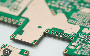
Then, enter the lamination process, which is one of the core steps in manufacturing multi-layer PCBs. The lamination process presses each layer of copper foil and insulation material together through high temperature and high pressure to form a whole.

This process requires precise control of temperature and pressure to ensure that the adhesion between the layers is strong and bubble-free.
Contact us for PCB quote now |

After lamination is completed, drilling is the next key step.

Drilling is used to create through holes for electrical connections and holes for mounting components. Modern PCB manufacturing usually uses CNC drilling machines to ensure the accuracy and consistency of hole positions.

After drilling is completed, the electroplating process is carried out to deposit copper on the hole wall to form a conductive channel. This step is particularly important for multi-layer PCBs because it ensures electrical connection between layers.

Subsequently, the pattern transfer and etching stage is entered.

First, the circuit pattern is transferred to the copper foil surface through a photolithography process. Then, a chemical etchant is used to remove the unprotected copper foil, leaving the desired circuit pattern. This process requires strict control to prevent over-etching or under-etching, which will affect the performance of the circuit.

After the circuit pattern is formed, surface treatment and pad plating are carried out. Common surface treatment methods include hot air leveling (HASL), chemical nickel gold plating (ENIG), etc.
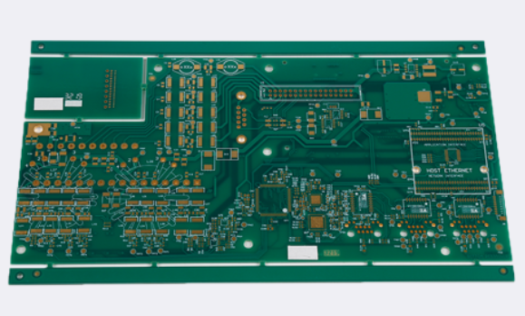
These treatment methods can improve welding performance and anti-oxidation ability. Next, the solder mask is applied, which can prevent short circuits during welding and protect the surface of the circuit board.

Finally, electrical testing and quality inspection are carried out. Electrical testing includes open circuit and short circuit tests to ensure that the electrical performance of the circuit board meets the design requirements. Quality inspection includes appearance inspection and size measurement to ensure that the appearance and size of the circuit board meet the standards.

In summary, the manufacturing process of 6-layer PCB involves multiple key steps and technical points, and each step requires precise control and strict management. Through scientific process flow and advanced manufacturing technology, the high quality and high reliability of 6-layer PCB can be ensured to meet the needs of various complex electronic devices.

Contact us for PCB quote now |

Post Tags: #6 layer pcb#6 layer pcb design#6 layer pcb manufacturing

Post navigation

Previous Previous
The Hidden Costs of PCB Manufacturing Equipment: Revealing the Price Tag Behind a High-Tech Factory
NextContinue
6 layer pcb motherboard

Search

Search

Products

  • HDI Multilayer PCB
  • Rigid Flex PCB
  • Flex pcb
  • High Frequency PCB
  • High speed pcb
  • Heavy copper PCB
  • Metal Core PCB
  • Ceramic PCB

Address

Andwin Circuits Co.,Limited
Email: sales@andwinpcb.com
Tel: +86 755 2832 9394
Fax:+86 755 2992  6717
ADD:1-2F-1217,HouDeQun Industrial park,
NanTing RD NO.56,ShaJing,BaoAn,Shenzhen 518104,GuangDong,China

Products

  • HDI Multilayer PCB
  • Rigid Flex PCB
  • Flex pcb
  • High Frequency PCB
  • High speed pcb
  • Heavy copper PCB
  • Metal Core PCB
  • Ceramic PCB

Technology

  • Blogs
  • Via in pad
  • PCB E-test
  • PCB stack up
  • Metal core PCB panelization
  • Controlled impedance PCB

CERTIFICATION

Certification >>


Copyright© 2003 - 2026 Andwin | All Rights Reserved | Powered by Andwin

Scroll to top
  • Home
  • Products
    • HDI multilayer PCB
    • Rigid Flex PCB
    • Flex pcb
    • Special PCB
      • High Frequency PCB
        • Rogers RO4350B PCB
        • Rogers RO4003 pcb
        • Rogers RO3003 PCB
        • Rogers 5880 PCB
        • DICLAD 527 PCB
        • Taconic TLX series
        • Taconic TLX-8 RF PCB
        • Taconic TLX-9 RF PCB
      • High speed pcb
        • Megtron 6 High Speed PCB
        • TU-872 SLK Sp High Speed
      • High TG PCB
        • SHENGYI SH260 PCB
        • ISOLA 370HR PCB
        • ISOLA IS410 PCB
        • ISOLA IS420 PCB
      • Heavy copper PCB
      • Copper coin pcb
      • Copper inlay PCB
    • Metal Core PCB
      • Copper core pcb
      • Aluminum PCB
      • 2 Layers Aluminum PCB
      • Direct thermal MCPCB
      • 2 Layers Direct Thermal
    • Ceramic PCB
      • DPC ceramic PCB
      • DBC ceramic PCB
      • Thick film Ceramic PCB
      • Al2O3 Alumina PCB
      • AIN ALN ceramic PCB
      • IGBT Ceramic PCB
  • Service
    • PCB Assembly
    • Quick turn PCB assembly
    • PCBA conformal coating
  • Industry
    • Telecommunication
    • IoT and Wireless
    • Industrial Control
    • Thermal management
    • Power and Energy
    • IC test board
    • Automative
    • Medical
  • Capability
    • Rigid PCB
    • Rigid flex PCB
    • Metal core PCB
    • PCB Assembly
  • Technology
    • Blogs
    • Via in pad
    • PCB E-test
    • PCB stack up
    • MCPCB panelization
    • Controlled impedance PCB
  • About
    • About us
    • Certification
    • Factory Tour
  • Contact
Search