
8 layer pcb
1.What is 8-layer pcb
8-layer PCB design plays a vital role in modern electronic engineering. Its advantages and application fields are wide and worthy of in-depth discussion. First, a significant advantage of the 8-layer PCB design is its high-density routing capabilities. Compared with PCBs with fewer layers, the 8-layer design can provide more wiring layers, which makes the design and implementation of complex circuits easier. By increasing the number of layers, designers can better manage signal paths and reduce signal interference and crosstalk, thereby improving the overall performance and reliability of the circuit
2.What is the structural composition of a 8-layer PCB?
Common substrates include FR4, ceramic, and polyimide. FR4 is a glass fiber reinforced epoxy resin that is widely used for its good mechanical properties and electrical insulation properties.
However, for high-frequency applications, ceramic substrates and polyimide are more suitable because they have lower dielectric constants and higher thermal stability.
Next, the selection of copper foil is also crucial. The thickness of copper foil is usually between 1oz and 3oz, and the specific selection depends on the current load and thermal conductivity requirements.
Thicker copper foil can carry more current, but it will also increase manufacturing costs and difficulty.
Therefore, the relationship between electrical performance and cost needs to be weighed during the design process.
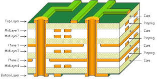
After material selection, structural design is another important link. 8-layer PCBs usually adopt a symmetrical structure to ensure the mechanical stability and electrical performance of the board. The common stacking sequence includes the reasonable distribution of signal layers, ground layers, and power layers. Usually, the outermost layer is the signal layer, and the middle layer alternately distributes the ground layer and the power layer. This design can not only effectively reduce electromagnetic interference, but also improve signal integrity.
In addition, the dielectric material between layers also needs to be carefully selected. The dielectric constant and thickness of the dielectric material directly affect the signal transmission speed and impedance matching. Commonly used dielectric materials include FR4, ceramics, and polyimide. For high-frequency applications, materials with low dielectric constants are more ideal because they can reduce signal delays and losses.
In the design process, thermal management is also a factor that cannot be ignored. The multi-layer structure of the 8-layer PCB makes it easy for heat to accumulate, affecting the stability and life of the circuit. Therefore, reasonable thermal design, including the use of heat dissipation holes, heat sinks, and thermal conductive materials, is the key to ensuring PCB reliability.
GET PCB MANUFACTURING AND ASSEMBLY QUOTE NOW!
3.What are the advantages of 8-layer PCB?
(1)high-density wiring capability.
(2)can effectively dissipate heat and extend the life of the device.
4.What are the disadvantages of 10-layer PCB?
(1)high cost
(2)the increased difficulty of repair and commissioning.
(3)The risk of defects such as misalignment, delamination, or incomplete connections increases with the number of layers.
First of all, a significant advantage of 8-layer PCB is its high-density wiring capability. Compared with single-layer or double-layer PCB, 8-layer PCB can accommodate more circuits and components.
This high-density routing capability enables designers to implement more complex circuit designs within limited space, thereby increasing the functionality and performance of electronic devices. In addition, 8-layer PCB can also effectively reduce signal interference and crosstalk.
Through reasonable stacking design, the signal layer and the ground layer can be isolated from each other, thereby reducing electromagnetic interference (EMI) and radio frequency interference (RFI), and improving signal integrity and stability.
Secondly, 8-layer PCB also performs well in thermal management. The multi-layer structure allows heat to be distributed more evenly, thereby avoiding the problem of local overheating.
This is especially important for high-power electronics, where overheating can cause component damage or performance degradation.
By adding thermally conductive materials between different layers, the 8-layer PCB can effectively dissipate heat and extend the life of the device.
However, 8-layer PCB also has some disadvantages.
The first is cost. Due to the complexity of the manufacturing process and the increase in materials, the production cost of 8-layer PCB is significantly higher than that of single-layer or double-layer PCB. This can be an important consideration for projects with limited budgets.
In addition, the design and manufacturing process of 8-layer PCB is also more complex and requires a higher level of technology and experience. This means designers and manufacturers need to invest more time and resources to ensure PCB quality and reliability.
Another potential disadvantage is the increased difficulty of repair and commissioning. Due to the complexity of 8-layer PCBs, once a failure occurs, locating and repairing the problem may require more time and expertise.
This can be a challenge for application scenarios that require rapid response and repair. In addition, the increased thickness of multi-layer PCBs may also have an impact on certain application scenarios.
For example, in some portable devices that require a thin and light design, an 8-layer PCB may not be as suitable as a single-layer or double-layer PCB.
To sum up, 8-layer PCB has significant advantages in high-density wiring, signal integrity and thermal management, but it also faces challenges of high cost, complex design and difficult maintenance.
When choosing whether to use an 8-layer PCB, designers need to consider the specific needs of the project, budget, and technical capabilities to make the most appropriate decision. By weighing these advantages and disadvantages, designers can better utilize the advantages of 8-layer PCBs while minimizing their potential disadvantages, thereby achieving the best electronic design results.
GET PCB AND ASSEMBLY SERVICE QUOTE NOW!
5.Application of 8-layer PCB
(1)widely used in many high-end electronic devices.
(2)in the field of computers and servers
(3)in medical equipment.
8-layer PCB design plays a vital role in modern electronic engineering. Its advantages and application fields are wide and worthy of in-depth discussion.
First, a significant advantage of the 8-layer PCB design is its high-density routing capabilities. Compared with PCBs with fewer layers, the 8-layer design can provide more wiring layers, which makes the design and implementation of complex circuits easier.
By increasing the number of layers, designers can better manage signal paths and reduce signal interference and crosstalk, thereby improving the overall performance and reliability of the circuit.
In addition, the 8-layer PCB design also has significant advantages in the distribution of power and ground planes.
The multi-layer design allows for more flexible distribution of power and ground planes, effectively reducing power supply noise and ground bounce noise.
This is especially important for high-frequency circuits and high-speed signal transmission because these circuits are more sensitive to noise. By optimizing the layout of power and ground planes, an 8-layer PCB can significantly improve the electrical performance and stability of the circuit.
Transitioning to the application field, 8-layer PCB design is widely used in many high-end electronic devices.
For example, in communication equipment, 8-layer PCB can support complex signal processing and high-speed data transmission requirements.
Communication equipment usually needs to handle large amounts of data and signals, so it requires high-density wiring and excellent electrical performance.
The 8-layer PCB design can meet these needs and ensure efficient operation and reliability of the equipment.
Likewise, in the field of computers and servers, 8-layer PCB design also plays an important role. Modern computers and servers need to process large amounts of data and perform complex computing tasks, which places high demands on circuit board performance.
The 8-layer PCB design not only provides sufficient wiring space, but also effectively manages the power and ground planes to ensure system stability and efficiency.
In addition, 8-layer PCB design also has important applications in medical equipment. Medical devices often require high-precision and high-reliability circuit design to ensure the safety and effectiveness of the device.
The 8-layer PCB design can provide high-density wiring and excellent electrical performance to meet the strict requirements of medical equipment for circuit boards.
To sum up, 8-layer PCB design has been widely used in fields such as communication equipment, computers and servers, and medical equipment due to its high-density wiring capabilities and excellent electrical performance.
By optimizing the layout of the power and ground planes, the 8-layer PCB design can significantly improve the performance and reliability of the circuit and meet the needs of modern electronic equipment for high-performance circuit boards. With the continuous development of electronic technology, 8-layer PCB design will continue to play an important role in more fields, providing a solid foundation for the development of electronic engineering.

Circuit board. Electronic computer hardware technology. Motherboard digital chip. Tech science background. Integrated communication processor. Information engineering component. (Circuit board. Electronic computer hardware technology. Motherboard digi