12 layer pcb
1.What is 12-layer pcb
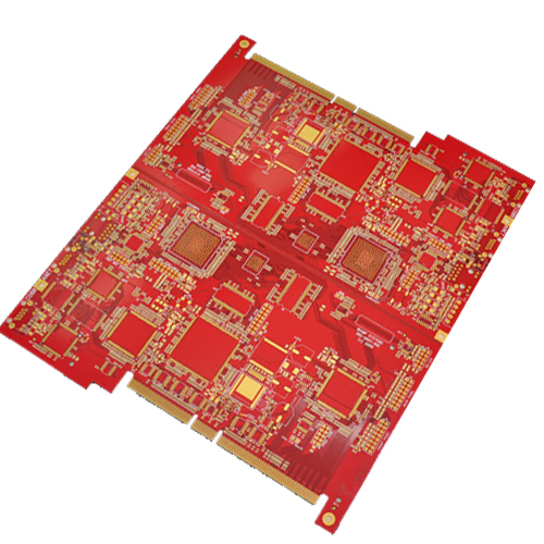
A 12-layer printed circuit board (PCB) represents a sophisticated and intricate component in the realm of electronics, embodying a significant leap in complexity and functionality compared to its simpler counterparts.
2.What is the structural composition of a 12-layer PCB?
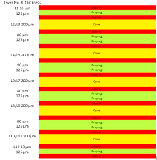
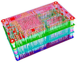
At its core, a 12-layer PCB consists of twelve distinct layers of conductive material, typically copper, separated by insulating layers known as dielectric materials. These layers are meticulously laminated together under high pressure and temperature to form a single, cohesive unit. The design of a 12-layer PCB is a meticulous process, requiring precise alignment and registration to ensure that the various layers interact correctly. This complexity allows for a higher density of components and interconnections, which is crucial for modern electronic devices that demand compactness and high performance.
GET PCB MANUFACTURING AND ASSEMBLY QUOTE NOW!
3.What are the advantages of 12-layer PCB?
(1)support high-density interconnections.
(2)improved thermal management
(3) support more complex circuitry
(4) the enhanced layer count provides greater flexibility in power distribution
4.What are the disadvantages of 12-layer PCB?
(1)increased cost
(2) the increased complexity of a 12-layer PCB can pose challenges in terms of testing and troubleshooting
One of the primary advantages of a 12-layer PCB is its ability to support high-density interconnections.
With multiple layers, designers can route more signals in a confined space, which is particularly beneficial for complex electronic devices such as smartphones, computers, and advanced medical equipment.
This high-density capability allows for the integration of more components, leading to enhanced functionality and performance.
Additionally, the multiple layers provide ample ground and power planes, which are essential for maintaining signal integrity and reducing electromagnetic interference (EMI). This results in more reliable and stable electronic devices.
Another significant advantage is the improved thermal management that a 12-layer PCB offers. The additional layers can be used to distribute heat more effectively, preventing hotspots and ensuring that components operate within their optimal temperature ranges.
This is particularly important in high-power applications where excessive heat can lead to component failure and reduced lifespan. Furthermore, the enhanced thermal management contributes to the overall durability and longevity of the electronic device.
However, despite these advantages, there are also notable disadvantages associated with 12-layer PCBs. One of the most prominent drawbacks is the increased cost.
The complexity of manufacturing a 12-layer PCB requires advanced fabrication techniques and materials, which can significantly drive up production costs
. This makes them less suitable for cost-sensitive applications or for products that are intended for mass production. Additionally, the design process for a 12-layer PCB is more intricate and time-consuming, requiring specialized knowledge and expertise. This can lead to longer development cycles and higher design costs.
Moreover, the increased complexity of a 12-layer PCB can pose challenges in terms of testing and troubleshooting.
Identifying and resolving issues in a multi-layered board can be more difficult compared to simpler PCBs, as faults may be buried within the inner layers. This necessitates the use of advanced diagnostic tools and techniques, which can further add to the overall cost and time required for development.
In conclusion, while 12-layer PCBs offer significant advantages in terms of high-density interconnections, improved signal integrity, and enhanced thermal management, they also come with notable disadvantages such as increased cost, complexity in design, and challenges in testing and troubleshooting.
Therefore, the decision to use a 12-layer PCB should be carefully considered based on the specific requirements and constraints of the project. By weighing the pros and cons, engineers and designers can make informed decisions that balance performance, reliability, and cost-effectiveness in their electronic
GET PCB AND ASSEMBLY SERVICE QUOTE NOW!
5.Application of 12-layer PCB
(1)used in In the telecommunications sector
(2)the medical field benefits from the precision and reliability of 12-layer PCBs
(3)In the automotive sector,
The applications of 12-layer PCBs extend across various industries, including telecommunications, aerospace, automotive, and medical devices. In telecommunications, for instance, 12-layer PCBs are used in high-frequency communication equipment such as routers, switches, and base stations.
These devices require reliable and high-speed data transmission, which is facilitated by the advanced capabilities of 12-layer PCBs. Similarly, in the aerospace industry, 12-layer PCBs are employed in avionics systems, where they contribute to the performance and reliability of critical flight control and navigation systems.
In the automotive sector, the increasing complexity of electronic systems in modern vehicles necessitates the use of multi-layer PCBs. Advanced driver-assistance systems (ADAS), infotainment systems, and electric vehicle power management systems all benefit from the enhanced performance and reliability offered by 12-layer PCBs.
Additionally, in the medical field, 12-layer PCBs are utilized in sophisticated diagnostic and monitoring equipment, where precision and reliability are paramount.
In conclusion, the advantages and applications of 12-layer PCBs in high-speed digital circuits are manifold. Their ability to support high-speed signal transmission, superior thermal management, design flexibility, and improved signal routing make them an essential component in a wide range of advanced electronic systems.
As technology continues to evolve, the demand for high-performance PCBs will only increase, further solidifying the importance of 12-layer PCBs in the realm of high-speed digital circuits