
Ten golden rules of PCB design
Despite the increasing integration of semiconductors, the availability of readily available systems-on-chip for many applications, and the increasing availability of powerful and ready-to-use development boards, many use cases still require the use of custom PCBs for electronic products.
Even a regular PCB can play a very important role in one-off development.
The PCB is the physical platform for design and the most flexible component for the original assembly of electronic system design. This article will introduce several golden rules of PCB design, which have remained largely unchanged since the birth of commercial PCB design 25 years ago and are widely applicable to various PCB design projects, whether for young electronic design engineers or more mature circuit board manufacturers
Article reference address:
The following content of this article introduces the ten most effective design rules that electronic design engineers should keep in mind and practice when using design software for PCB layout design and commercial manufacturing. Engineers do not need to follow these rules in chronological order or relative importance, just following them all can greatly change product design.
Rule 1: Choose the right grid – Set and always use the grid spacing that will fit the most components. While multiple grids may seem obvious, engineers can avoid spacing challenges and maximize board utilization by giving a little more thought early in the PCB layout design process. Since many devices come in multiple package sizes, engineers should use the product that works best for their design. In addition, polygons are critical to board copper pouring, and multiple grid boards generally produce polygon fill deviations when pouring polygons, which, while not as standard as those based on a single grid, can provide board life that exceeds requirements.
Rule 2: Keep paths short and direct. This may sound simple, but it should be kept in mind at every stage, even if it means changing the board layout to optimize trace lengths. This is especially true for analog and high-speed digital circuits, where system performance is always partially limited by impedance and parasitics.
Rule 3: Use power planes to manage the distribution of power and ground lines whenever possible. Power plane pouring is the quickest and easiest option for most PCB design software. By connecting a large number of wires in common, it ensures that the most efficient current is delivered with the least impedance or voltage drop, while providing ample ground return paths. If possible, run multiple supply lines in the same area of the board and confirm that the ground plane covers most of a layer of the PCB, which can help to interact with lines running on adjacent layers.
Rule 4: Group related components with required test points. For example, placing discrete components required for an OpAmp close to the device so that bypass capacitors and resistors can work with it on the same ground helps optimize the trace lengths mentioned in Rule 2, while also making testing and troubleshooting easier.
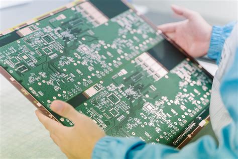
Rule 5: Repeat the required board on another larger board for PCB assembly. Choosing the size that best suits the equipment used by the manufacturer can help reduce prototyping and manufacturing costs. Start by laying out the board on a panel, contact the board manufacturer to get their preferred size specifications for each panel, then modify your design specifications and try to repeat your design multiple times within these panel sizes.
Rule 6: Consolidate component values. As a designer, you will choose discrete components with higher or lower values but the same performance. By consolidating within a smaller range of standard values, you can simplify the bill of materials and potentially reduce costs. If you have a range of PCBs based on preferred component values, you will be better placed to make the right inventory management decisions in the long run.
Rule 7: Perform design rule checks (DRCs) as often as possible. Although it only takes a short time to run the DRC function on your PCB software, in a more complex design environment, you can save a lot of time by always performing checks during the design process, which is a good habit to maintain. Every routing decision is critical, and performing DRCs can remind you of the most important routing at any time.
Rule 8: Use silkscreen flexibly. Silkscreen can be used to mark a variety of useful information for future use by board manufacturers, service or test engineers, installers, or equipment commissioning personnel. Not only should clear function and test point labels be marked, but also component and connector orientation should be marked whenever possible, even if these notes are printed on the underside of the components used on the board (after the board is assembled). The full use of silkscreen technology on both the upper and lower surfaces of the board can reduce duplication of work and streamline the production process.
Rule 9: Decoupling capacitors are mandatory. Don’t try to optimize your design by avoiding decoupling power lines and relying on the extreme values in the component datasheet. Capacitors are cheap and rugged, so you can spend as much time as possible assembling them well, while following Rule 6 and using a standard range of values to keep your inventory neat.
Rule 10: Generate PCB manufacturing parameters and verify before submitting them for production. While most board manufacturers will be happy to download and verify them for you, it is best to export the Gerber files yourself and use a free viewer to check that they are what you expected to avoid misunderstandings. By verifying them yourself, you may even find some careless mistakes and avoid the cost of completing production to the wrong parameters.
As circuit designs are shared more and more, and internal teams rely more and more on reference designs, basic rules like these will continue to be a feature of printed circuit board design, and we believe this is very important for PCB design. With these basic rules clear, developers have great flexibility to increase the value of their products and get the most from the boards they manufacture. Even for novice board designers, just keeping these basic rules in mind can speed up the learning process and increase confidence.