
About the production process of PCB/FPC blind hole buried hole board
I. Overview:
Blind hole and buried hole board are mainly used for high-density, small micro-hole board production, the purpose is to save circuit space, so as to achieve the purpose of reducing the volume of PCB, such as mobile phone board,
II. Classification:
I). Laser drilling,
- Reasons for laser drilling:
a. Customer information requires laser drilling;
b Because the blind hole diameter is very small <= 6MIL, laser drilling is required.
c. Special blind buried holes, such as blind holes from L1 to L2, and buried holes from L2 to L3, must be drilled with laser.
- Principle of laser drilling:
Laser drilling uses the board to absorb the heat of the laser to vaporize or dissolve the board into holes, so the board must be light-absorbing, so the general RCC material, because there is no glass fiber cloth in RCC, will not reflect light .
- Introduction to RCC materials:
RCC materials are resin-coated copper foil:
It is formed by coating a layer of resin with unique properties on the rough surface of electrolytic copper foil.
Currently, our company has three suppliers for RCC materials: Shengyi, Mitsui, and LG.
Material: Resin thickness 50 65 70 75 80 (um), etc.
Copper foil thickness 12 18 (um), etc.
RCC materials have high TG and low TG materials, and the dielectric constant is smaller than the normal FR4. For example, the dielectric constant of S6018 of Guangdong Shengyi Company is 3.8, so pay attention when there is impedance control.
For other specific reference materials, please ask the PE and RD departments.
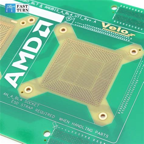
- Requirements for tool production for laser drilling:
A). It is difficult for the laser to burn through the copper foil, so before laser drilling, a Cu Clearance equal to the completed aperture must be etched out at the blind hole position.
B). The positioning mark for laser drilling is added to the L2/LN-1 layer, It should be noted on the MI film modification page.
C). The film for etching blind holes must be made with LDI, and the size of LDI board should be used for cutting.
- Features of production process:
A). When the total number of circuit layers is N, L2-Ln-1 layers are first made according to the normal board process,
B). After pressing the board and gonging the periphery, the process is changed to:
—> Drill LDI positioning holes—> Dry film—> Etch blind holes—> Laser drilling—> Drill through holes
—> Copper deposition—-(normal process).
- Other considerations:
A). Since RCC materials have not passed UL certification, this type of board will not be marked with UL for the time being.
B). Regarding the layout structure on MI, in order to avoid treating this type of layout containing RCC materials as a false layer layout (because the film room makes film false layers differently from normal boards), when drawing the layout structure, we must pay attention to the separation of RCC materials from L2 or Ln-1 layers, such as SR2711/01 layout:
C). IPC-6016 is the HDI board standard:
Laser blind hole wall copper thickness: 0.4mil (min).
Solder ring requirements: Tangent allowed
If the PAD size is less than 5mil larger than the hole diameter, it is recommended to add TEARDROP
D). Board edge>=0.8”
II). Mechanical drilling of blind/buried vias:
- Scope of application:
When the drill size is >= 0.20mm, mechanical drilling can be considered;
- About the electroplating method of blind buried vias (refer to RD Notice TSFMRD-113):
A). Under normal circumstances, the copper surface of any layer of circuit can only be electroplated once + once for pattern plating;
B). Under normal circumstances, after the full press process is completed, the board thickness is >= 80MIL, and the through hole needs to be electroplated + pattern plating. Therefore, the outer layer of the board cannot be electroplated when the blind hole is electroplated.
C). After the above two conditions are met, the electroplating of the blind hole is carried out as follows:
I). When the width of the outer layer line is greater than 6MIL, and the thickness of the through hole is less than 80MIL, the outer layer of the board can be electroplated in the blind hole plating
II). When the width of the outer layer line is greater than 6MIL, However, when the through-hole board thickness is greater than 80MIL, the outer board surface needs to be protected by a film during blind hole electroplating;
III). When the outer line width is less than 6MIL, and the through-hole board thickness is greater than or equal to 80MIL,
the outer board surface needs to be protected by a film during blind hole electroplating;
- Filming method:
1) When the blind hole aspect ratio is less than or equal to 0.8 (L/D), the outer board surface is exposed with a dry film, and the inner blind hole board surface is electroplated on the whole board,
2) When the blind hole aspect ratio is greater than or equal to 0.8 (L/D), the outer board surface is exposed with a dry film, and a plating exposure point film or LDI exposure is required, and the inner blind hole board surface is electroplated on the whole board.
4.Blind hole exposure method:
1) When the blind hole is less than or equal to 0.4MM (16MIL), use LDI to expose the blind hole,
2) When the blind hole is greater than 0.4MM (16MIL), use film to expose blind holes,
5.Buried hole filming method:
1) When the line width of the buried hole surface is <=4MIL, the buried hole board surface needs to be filmed and exposed,
2) When the line width of the buried hole surface is >4MIL, the buried hole board surface is directly electroplated,
6.Notes:
1) L/D in aspect ratio: L=medium thickness+copper thickness, D=blind hole/buried hole diameter.
2) Blind hole/buried hole electroplating film:
- The diameter of the exposure point D=D-6 (MIL).
*The exposure point film plus the alignment point, its coordinates are consistent with the peripheral reference hole.
3) Blind holes that need to be filmed generally use pulse current (AC) during electroplating.