
Analysis of the electroplating sealing/filling process of ceramic substrates
Electroplated sealing is a commonly used printed circuit board manufacturing process for filling and sealing vias (through holes) to enhance conductivity and protection. In the printed circuit board manufacturing process, vias are channels used to connect different circuit layers. The purpose of electroplated sealing is to form a layer of metal or conductive material deposition inside the via hole, so that the inner wall of the via hole is filled with conductive substances, thereby enhancing the conductivity and providing a better sealing effect.
1.The circuit board electroplating sealing process brings many advantages in the product manufacturing process:
(1)Improve circuit reliability:
The circuit board electroplating sealing process can effectively seal the holes and prevent electrical short circuits between metal layers on the circuit board. This helps to improve the reliability and stability of the circuit board and reduce the risk of circuit failure and damage.
(2)Enhance circuit performance:
Through the electroplating sealing process, better circuit connection and conductivity can be achieved. Electroplating filling holes can provide more stable and reliable circuit connections, reduce signal loss and impedance mismatch problems, and thus improve circuit performance and work efficiency.
(3)Improve welding quality:
The circuit board electroplating sealing process can also improve welding quality. The sealing process can form a flat and smooth surface in the hole, providing a better foundation for welding. This can improve the reliability and strength of welding and reduce the occurrence of welding defects and cold welding.
(4)Strengthen mechanical strength:
The electroplating sealing process can improve the mechanical strength and durability of the circuit board. Filling the holes can increase the thickness and firmness of the circuit board, improve its resistance to bending and vibration, and reduce the risk of mechanical damage and breakage of the circuit board during use.
(5)Facilitate assembly and installation:
The circuit board electroplating sealing process can make the assembly and installation process more convenient and efficient. Filling the holes can provide a more stable surface and connection points, making the installation of components easier and more accurate. In addition, electroplating sealing can also provide better protection and reduce damage and loss of components during installation.
Overall, the circuit board electroplating sealing process can improve circuit reliability, enhance circuit performance, improve welding quality, strengthen mechanical strength, and facilitate assembly and installation. These advantages can significantly improve the quality and reliability of products while reducing the risks and costs in the manufacturing process.
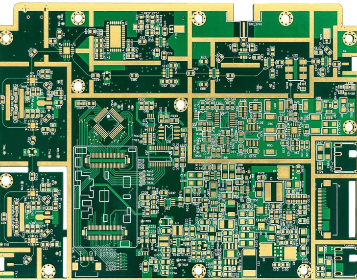
2.Although the PCB electroplating sealing process has many advantages, there are also some potential risks or disadvantages, including the following:
- Increased cost: The PCB electroplating sealing process requires additional processes and materials, such as filling materials and chemicals used in the electroplating process. This may increase manufacturing costs and affect the overall economic efficiency of the product.
- Long-term reliability: Although the electroplating sealing process can improve the reliability of the circuit board, the filling materials and electroplating layers may be affected by factors such as thermal expansion and contraction, humidity, and corrosion under long-term use and environmental changes. This may cause the filling materials to loosen, fall off, or damage the electroplating layer, thereby reducing the reliability of the circuit board.
- Process complexity: The PCB electroplating sealing process is more complicated than the conventional process. It involves multiple steps and parameter control such as hole preparation, selection and construction of filling materials, and control of the electroplating process. This may require higher process skills and equipment to ensure the accuracy and stability of the process.
- Increase of process: Add sealing process, and add blocking film for slightly larger holes to ensure the sealing effect. After sealing, it is necessary to go through copper scraping, grinding, polishing and other steps to ensure the flatness of the sealing surface.
- Environmental impact: The chemicals used in the electroplating sealing process may have a certain impact on the environment. For example, wastewater and waste liquid may be generated during the electroplating process, which need to be properly treated and handled. In addition, there may be environmentally harmful components in the filling material, which need to be properly managed and handled.
When considering the circuit board electroplating sealing process, these potential hidden dangers or shortcomings need to be comprehensively considered, and the pros and cons should be weighed according to specific needs and application scenarios. When implementing the process, appropriate quality control and environmental management measures are crucial to ensure the best process results and product reliability.
3.Acceptance Standards
Based on the standard: IPC-600-J3.3.20: Electroplated copper-filled microvias (blind and buried)
Depressions and protrusions: The requirements for protrusions (bumps) and depressions (pits) of copper-filled blind microvias should be determined by negotiation between the supply and demand parties. There are no requirements for protrusions and depressions of copper-filled busy microvias. The specific judgment is based on the customer’s procurement documents or customer standards.