
Skip to content
Andwin Circuits
  • Home
  • ProductsExpand
    • HDI multilayer PCB
    • Rigid Flex PCB
    • Flex pcb
    • Special PCBExpand
      • High Frequency PCBExpand
        • Rogers RO4350B PCB
        • Rogers RO4003 pcb
        • Rogers RO3003 PCB
        • Rogers 5880 PCB
        • DICLAD 527 PCB
        • Taconic TLX series
        • Taconic TLX-8 RF PCB
        • Taconic TLX-9 RF PCB
      • High speed pcbExpand
        • Megtron 6 High Speed PCB
        • TU-872 SLK Sp High Speed
      • High TG PCBExpand
        • SHENGYI SH260 PCB
        • ISOLA 370HR PCB
        • ISOLA IS410 PCB
        • ISOLA IS420 PCB
      • Heavy copper PCB
      • Copper coin pcb
      • Copper inlay PCB
    • Metal Core PCBExpand
      • Copper core pcb
      • Aluminum PCB
      • 2 Layers Aluminum PCB
      • Direct thermal MCPCB
      • 2 Layers Direct Thermal
    • Ceramic PCBExpand
      • DPC ceramic PCB
      • DBC ceramic PCB
      • Thick film Ceramic PCB
      • Al2O3 Alumina PCB
      • AIN ALN ceramic PCB
      • IGBT Ceramic PCB
  • ServiceExpand
    • PCB Assembly
    • Quick turn PCB assembly
    • PCBA conformal coating
  • IndustryExpand
    • Telecommunication
    • IoT and Wireless
    • Industrial Control
    • Thermal management
    • Power and Energy
    • IC test board
    • Automative
    • Medical
  • CapabilityExpand
    • Rigid PCB
    • Rigid flex PCB
    • Metal core PCB
    • PCB Assembly
  • TechnologyExpand
    • Blogs
    • Via in pad
    • PCB E-test
    • PCB stack up
    • MCPCB panelization
    • Controlled impedance PCB
  • AboutExpand
    • About us
    • Certification
    • Factory Tour
  • Contact
Andwin Circuits
Home / How to distinguish via cover oil and via opening in the PCB printing process

How to distinguish via cover oil and via opening in the PCB printing process

ByGrace March 7, 2025March 5, 2025

Regarding the point of “via cover oil” and “via opening” (the difference between the usage of VIA and PAD), many customers and design engineers often ask what this means when placing orders on the system, and which option should I choose for my file? The following is an explanation of this issue:

I often encounter such problems.

The design is seriously non-standard. It is impossible to distinguish the usage of pad and via. Sometimes the conductive hole is processed with the attribute of pad, and sometimes the key hole is processed with the attribute of via. The design of VIA attribute and PAD attribute is confusing, resulting in incorrect processing. This is also one of the problems that often cause complaints. For circuit board production factories, when processing CAM data, some film processing engineers, because of the non-standard design files of customers, make mistakes and help customers modify the files to make the non-standard design correct. They process the engineering data based on their own experience, which leads to and contributes to the non-standard design of customers.

Jieduobang hereby explains: What you did right last time does not mean that your file is correct! All engineers must pay attention to the design standards and specifications! Jieduobang will once again strictly require all film processing engineers to keep the status quo of customer files as much as possible! Try to handle it according to the design specifications and standards as much as possible, and do not handle it according to the so-called experience! Reflect the problem, so that it can be a reference for all design engineers to improve the design quality and reduce the occurrence of problems!
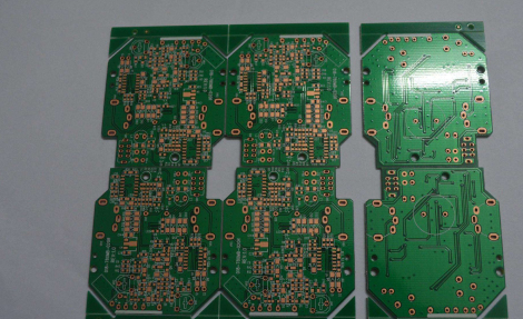
Mixing pads and vias leads to problems

  1. When your file is pads or protel, send it to the factory and ask for via cover oil. Be sure to check carefully whether your plug-in hole (pad) also uses via, otherwise your plug-in hole will also be covered with green oil, which will lead to welding failure. Point of dispute: The plug-in hole must be sprayed with tin. How do you cover it? How do I use it? When you say this, please check the file. Is it designed with pads or vias!
  2. When your file is pads or protel, send the file to the factory and place an order requiring via cover oil. Many customers use pad (plug-in hole) to indicate conductive holes, which leads to your conductive holes opening windows. Maybe you want via cover oil. At that time, the point of dispute may be, what I want is conductive hole cover oil, why is it opened? Then please check your file design! If it is via, treat it as via, if it is pad, treat it as pad! Because no one will know that it is a conductive hole and that is a plug-in hole, and via and pad are the only identifications, please be clear!
  3. During the conversion process of via, problems may occur due to non-standard design or unclear setting rules for gerber conversion. When you send a gerber file, the factory manufacturer cannot distinguish which are vias and which are key holes. The only way to identify is to process according to the file. If there is a solder layer, there will be a window! Point of dispute: I want a via cover oil, and you open a window for me now, I may cause a short circuit, so please check your file. The gerber you issued is a film file. The factory has no way to check whether yours is a conductive hole or a key hole. Please check the gerber file to see if there is a solder layer. If there is, open a window, if not, cover with oil
  4. How to design a via cover oil in protel or pads! – This is the most standard practice. If the design is standard, there will be no mistakes!

In protel, there is a tenting option in the via attribute. If you check it, it must be covered with oil, so what you transfer will be all covered with oil. In pads, the pads transfer file is to cover the via. The method is: when outputting the soldermask, that is, the solder mask layer, just check the upper solder mask top —— the via below, which means that all vias are opened. If it is not checked, the vias are covered with oil. In summary: pads are made according to pads, which are plug-in holes. For vias, you have two choices. If you provide the original file, you can choose when placing an order. If you provide the gerber file, you must check whether the gerber file meets your requirements!

Contact us for PCB quote now |
Post Tags: #aluminum clad pcb#aluminum core pcb#aluminum core pcb led#aluminum pcb#assemble pcb

Post navigation

Previous Previous
Why Choose Lever Terminal Blocks in PCB Circuits
NextContinue
Optimizing PCB Via Design: A Comprehensive Guide

Search

Search

Products

  • HDI Multilayer PCB
  • Rigid Flex PCB
  • Flex pcb
  • High Frequency PCB
  • High speed pcb
  • Heavy copper PCB
  • Metal Core PCB
  • Ceramic PCB

Address

Andwin Circuits Co.,Limited
Email: sales@andwinpcb.com
Tel: +86 755 2832 9394
Fax:+86 755 2992  6717
ADD:1-2F-1217,HouDeQun Industrial park,
NanTing RD NO.56,ShaJing,BaoAn,Shenzhen 518104,GuangDong,China

Products

  • HDI Multilayer PCB
  • Rigid Flex PCB
  • Flex pcb
  • High Frequency PCB
  • High speed pcb
  • Heavy copper PCB
  • Metal Core PCB
  • Ceramic PCB

Technology

  • Blogs
  • Via in pad
  • PCB E-test
  • PCB stack up
  • Metal core PCB panelization
  • Controlled impedance PCB

CERTIFICATION

Certification >>


Copyright© 2003 - 2026 Andwin | All Rights Reserved | Powered by Andwin

Scroll to top
  • Home
  • Products
    • HDI multilayer PCB
    • Rigid Flex PCB
    • Flex pcb
    • Special PCB
      • High Frequency PCB
        • Rogers RO4350B PCB
        • Rogers RO4003 pcb
        • Rogers RO3003 PCB
        • Rogers 5880 PCB
        • DICLAD 527 PCB
        • Taconic TLX series
        • Taconic TLX-8 RF PCB
        • Taconic TLX-9 RF PCB
      • High speed pcb
        • Megtron 6 High Speed PCB
        • TU-872 SLK Sp High Speed
      • High TG PCB
        • SHENGYI SH260 PCB
        • ISOLA 370HR PCB
        • ISOLA IS410 PCB
        • ISOLA IS420 PCB
      • Heavy copper PCB
      • Copper coin pcb
      • Copper inlay PCB
    • Metal Core PCB
      • Copper core pcb
      • Aluminum PCB
      • 2 Layers Aluminum PCB
      • Direct thermal MCPCB
      • 2 Layers Direct Thermal
    • Ceramic PCB
      • DPC ceramic PCB
      • DBC ceramic PCB
      • Thick film Ceramic PCB
      • Al2O3 Alumina PCB
      • AIN ALN ceramic PCB
      • IGBT Ceramic PCB
  • Service
    • PCB Assembly
    • Quick turn PCB assembly
    • PCBA conformal coating
  • Industry
    • Telecommunication
    • IoT and Wireless
    • Industrial Control
    • Thermal management
    • Power and Energy
    • IC test board
    • Automative
    • Medical
  • Capability
    • Rigid PCB
    • Rigid flex PCB
    • Metal core PCB
    • PCB Assembly
  • Technology
    • Blogs
    • Via in pad
    • PCB E-test
    • PCB stack up
    • MCPCB panelization
    • Controlled impedance PCB
  • About
    • About us
    • Certification
    • Factory Tour
  • Contact
Search