
PCB Gerber File Generation: A Comprehensive Guide
Introduction
Printed Circuit Board (PCB) design is a crucial step in electronics manufacturing, and the Gerber file format serves as the industry standard for transferring PCB design data to fabrication facilities. Gerber files contain all the necessary information—such as copper layers, solder mask, silkscreen, and drill data—required to manufacture a PCB.
Generating accurate Gerber files is essential because any errors can lead to manufacturing defects, increased costs, and project delays. This article provides a detailed guide on PCB Gerber file generation, covering its importance, file formats, generation process, and best practices.
1. What Are Gerber Files?
Gerber files are open ASCII vector format files used to describe PCB images, including copper traces, pads, vias, solder masks, and silkscreen layers. They were originally developed by Gerber Systems Corp. (now Ucamco) and are standardized under RS-274X (Extended Gerber), which is the most widely used format today.
Key Gerber File Layers
A typical PCB design consists of multiple layers, each represented by a separate Gerber file. The most common layers include:
- Copper Layers (Top and Bottom): Conductive traces and pads.
- Solder Mask Layers: Protective coating over copper to prevent short circuits.
- Silkscreen Layers: Component labels and logos.
- Drill Files (Excellon format): Hole locations and sizes for through-hole components and vias.
- Board Outline (Mechanical Layer): Defines the PCB’s physical dimensions.
2. Why Are Gerber Files Important?
Gerber files act as the “blueprint” for PCB fabrication. Their accuracy ensures:
- Precise Manufacturing: Ensures that the PCB manufacturer correctly interprets the design.
- Compatibility: Standardized format accepted by all PCB fabrication houses.
- Error Reduction: Minimizes misinterpretation between designers and manufacturers.
- Design Verification: Allows designers to review the final output before production.
Incorrect Gerber files can lead to issues like misaligned layers, missing traces, or incorrect drill holes, resulting in non-functional boards.
3. Gerber File Generation Process
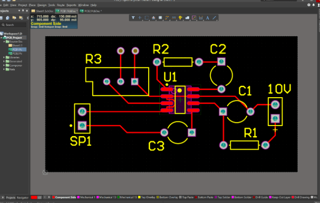
Generating Gerber files involves exporting design data from PCB design software (such as Altium Designer, KiCad, Eagle, or OrCAD) in the correct format. Below is a step-by-step guide:
Step 1: Finalize PCB Design
Before generating Gerber files, ensure that:
- All traces, components, and layers are correctly placed.
- Design Rule Checks (DRC) are performed to avoid errors.
- The board outline is properly defined.
Step 2: Configure Gerber Export Settings
In your PCB design software, access the Gerber generation tool and configure the following:
- File Format: RS-274X (Extended Gerber).
- Units: Millimeters (mm) or Inches (mil).
- Coordinate Format: Absolute or incremental (usually absolute).
- Aperture Settings: Automatic or custom (modern software typically handles this automatically).
Step 3: Select Layers to Export
Choose which layers to include in the Gerber files. Common selections:
- Top Copper (GTL)
- Bottom Copper (GBL)
- Top Solder Mask (GTS)
- Bottom Solder Mask (GBS)
- Top Silkscreen (GTO)
- Bottom Silkscreen (GBO)
- Board Outline (GKO/GML)
Step 4: Generate Drill Files
Drill files (in Excellon format) specify hole locations and sizes. Ensure:
- Drill File Format: Excellon 1 or 2.
- Units and Precision: Match the Gerber file settings.
- Include NC Drill File: For automated drilling machines.
Step 5: Verify Gerber Files
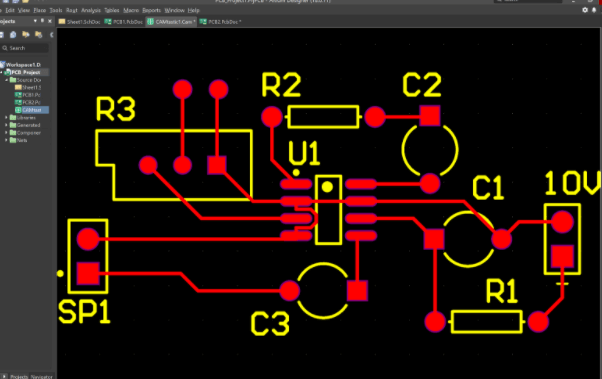
Before sending files to the manufacturer, use a Gerber viewer (such as GerberLogix, ViewMate, or KiCad’s GerbView) to check for:
- Missing or misaligned layers.
- Incorrect pad sizes or trace widths.
- Drill file alignment with copper layers.
4. Common Gerber File Formats
- RS-274D (Standard Gerber): Older format requiring an aperture list.
- RS-274X (Extended Gerber): Modern standard with embedded apertures, eliminating the need for separate files.
- Excellon (Drill Files): Specifies hole locations and sizes.
- ODB++: An alternative to Gerber, containing all data in a single structured file (used by some manufacturers).
Most PCB manufacturers prefer RS-274X due to its reliability and ease of use.
5. Best Practices for Gerber File Generation
To avoid manufacturing errors, follow these best practices:
1. Use Consistent Naming Conventions
Standardize file names (e.g., TopLayer.GTL, BottomLayer.GBL) to avoid confusion.
2. Include a Readme File
Provide a document explaining:
- Layer stack-up.
- Special manufacturing instructions.
- Any non-standard requirements.
3. Verify with a Gerber Viewer
Always inspect files before submission to catch errors early.
4. Check Design Rules with the Manufacturer
Different PCB manufacturers may have specific requirements (e.g., minimum trace width, hole sizes).
5. Avoid Non-Standard Features
Some fabrication houses may not support certain features (e.g., custom apertures in RS-274D).
6. Double-Cetch Drill Files
Ensure drill files match the Gerber layers to prevent misaligned holes.
6. Common Mistakes and How to Avoid Them
| Mistake | Solution |
|---|---|
| Missing layers | Double-check layer selection before export. |
| Incorrect units (mm vs. mil) | Confirm units with the manufacturer. |
| Misaligned drill files | Verify drill file alignment in a Gerber viewer. |
| Overlapping silkscreen on pads | Adjust silkscreen placement in the design. |
| Incomplete board outline | Ensure the mechanical layer is correctly defined. |
7. Conclusion
Generating accurate Gerber files is a critical step in PCB manufacturing. By following standardized procedures, verifying files before submission, and adhering to manufacturer guidelines, designers can ensure smooth and error-free PCB production.
Modern PCB design tools have simplified Gerber generation, but manual verification remains essential. Always use a Gerber viewer to inspect files and communicate clearly with your fabrication house to avoid costly mistakes. With proper attention to detail, you can achieve high-quality PCB manufacturing every time.