
Ceramic Antenna vs PCB Antenna: A Comprehensive Comparison
Introduction
In the rapidly evolving world of wireless communication, antenna design plays a critical role in determining the performance, reliability, and form factor of connected devices. Two popular antenna solutions that have emerged for compact wireless applications are ceramic antennas and PCB (Printed Circuit Board) antennas. This 2000-word article provides a detailed comparison between these two antenna types, examining their design principles, performance characteristics, manufacturing considerations, and optimal use cases.
Understanding Ceramic Antennas
Ceramic antennas are a type of chip antenna that utilize high-permittivity ceramic materials as their substrate. These compact components are typically surface-mounted devices (SMDs) that integrate directly onto a PCB.
Construction and Materials
Ceramic antennas consist of:
- High-dielectric ceramic material (typically with εr ranging from 10 to 40)
- Conductive traces printed or embedded within the ceramic
- External electrodes for soldering to the host PCB
- Often include a ground plane as part of their structure
The high dielectric constant allows for significant size reduction compared to antennas in free space, as wavelength in the material is reduced by a factor of √εr.
Performance Characteristics
- Size: Extremely compact, often just a few millimeters in each dimension
- Frequency Range: Typically designed for specific bands (2.4GHz, 5GHz, etc.)
- Bandwidth: Generally narrower bandwidth compared to PCB antennas
- Efficiency: Ranges from 30% to 70%, depending on design and implementation
- Gain: Typically lower gain due to small physical size
Advantages
- Miniaturization: Smallest form factor available for many applications
- Consistency: Tight manufacturing tolerances ensure consistent performance
- Integration: Simple surface-mount assembly process
- Isolation: Less affected by nearby components due to contained fields
Disadvantages
- Narrow bandwidth: May not cover entire required spectrum
- Lower efficiency: Energy loss in ceramic material
- Fixed performance: Limited tuning options after manufacturing
- Cost: More expensive than PCB trace antennas
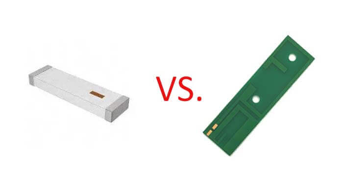
Understanding PCB Antennas
PCB antennas are conductive traces patterned directly onto the printed circuit board of the device. These antennas leverage the existing board substrate (typically FR4) as their dielectric material.
Common PCB Antenna Types
- Inverted-F Antenna (IFA)
- Planar Inverted-F Antenna (PIFA)
- Meandered Dipole
- Patch Antenna
- Loop Antenna
Construction and Materials
PCB antennas consist of:
- Copper traces etched onto the PCB substrate
- FR4 (εr ≈ 4.3) or high-frequency laminates (Rogers, Taconic, etc.)
- Carefully designed ground planes
- Possible matching networks using discrete components
Performance Characteristics
- Size: Larger than ceramic antennas for same frequency
- Frequency Range: Can be designed for multiple bands
- Bandwidth: Generally wider bandwidth capabilities
- Efficiency: Typically 50-80% on FR4, higher with RF substrates
- Gain: Can achieve higher gain with proper design
Advantages
- Cost-effective: Uses existing PCB real estate
- Design flexibility: Can be tuned during development
- Wide bandwidth: Can cover multiple bands or wider ranges
- Higher efficiency: Less dielectric loss than ceramic
- Integration: No additional components needed
Disadvantages
- Larger size: Requires more board space
- Sensitivity: Performance affected by nearby components
- Manufacturing variance: PCB tolerances affect performance
- Design complexity: Requires careful RF design expertise
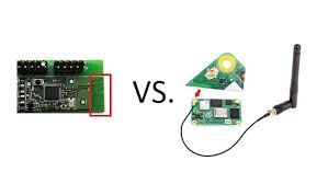
Detailed Comparison
1. Size and Form Factor
Ceramic Antenna:
- Typical sizes range from 1.0×0.5mm to 10×3mm
- 3D structure allows for compact volume
- Ideal for extremely space-constrained applications
PCB Antenna:
- Typically requires 10×5mm to 30×10mm area
- 2D planar structure consumes board area
- Needs keep-out zones around the antenna
Winner for miniaturization: Ceramic antenna
2. Electrical Performance
Ceramic Antenna:
- Narrow bandwidth (often <5% of center frequency)
- Moderate radiation efficiency (30-70%)
- Consistent performance across units
- Limited gain due to small size
PCB Antenna:
- Wider bandwidth possible (up to 10-15% of center frequency)
- Higher efficiency (50-80% on FR4, up to 90% on RF substrates)
- More design flexibility for gain optimization
- Performance varies with PCB manufacturing
Winner for performance: PCB antenna
3. Design and Implementation
Ceramic Antenna:
- Plug-and-play solution
- Minimal RF design expertise required
- Limited tuning options (external matching network)
- Requires proper ground plane design
PCB Antenna:
- Requires RF design expertise
- Allows for iterative tuning and optimization
- Can be customized for specific requirements
- More sensitive to board layout and components
Winner for ease of use: Ceramic antenna
4. Cost Considerations
Ceramic Antenna:
- Unit cost: $0.10-$1.00 in volume
- Additional cost for matching components
- No additional PCB area cost
PCB Antenna:
- No additional component cost
- Uses existing PCB layers
- Higher design and testing costs
- Opportunity cost of board space
Winner for cost: PCB antenna in most cases
5. Manufacturing and Reliability
Ceramic Antenna:
- Precise manufacturing controls
- Consistent performance unit-to-unit
- Robust mechanical structure
- Limited thermal expansion issues
PCB Antenna:
- Subject to PCB manufacturing tolerances
- Performance varies with copper thickness, etching
- Potential for delamination in harsh environments
- More sensitive to assembly variations
Winner for consistency: Ceramic antenna
Application-Specific Considerations
Best Applications for Ceramic Antennas
- Ultra-compact devices: Wearables, small IoT sensors
- High-volume production: Where consistency is critical
- Multi-band solutions: Some ceramic antennas cover multiple bands
- Applications with limited RF expertise: Faster time-to-market
Best Applications for PCB Antennas
- Cost-sensitive high-volume products: Consumer electronics
- Wideband requirements: WiFi, broadband applications
- Devices with available board space: Larger IoT devices, routers
- Custom performance requirements: Specific radiation patterns
Performance Optimization Techniques
Ceramic Antenna Optimization
- Ground plane design: Critical for proper performance
- Matching networks: Can improve bandwidth and efficiency
- Placement: Keep away from metal components
- Board thickness: Affects antenna performance
PCB Antenna Optimization
- Substrate selection: High-frequency laminates improve performance
- 3D structure: Using multiple PCB layers
- Matching circuits: Can be integrated into design
- Simulation: Essential for optimal performance
Future Trends
- Hybrid solutions: Combining ceramic and PCB elements
- Advanced materials: Higher efficiency ceramics
- 3D printed antennas: For customized solutions
- AI-optimized designs: For space-constrained applications
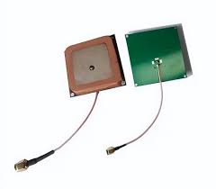
Conclusion
The choice between ceramic antennas and PCB antennas depends on specific application requirements:
- Choose ceramic antennas when: Size is the primary constraint, consistency is critical, or RF design resources are limited.
- Choose PCB antennas when: Cost is paramount, bandwidth requirements are high, or board space is available for optimization.
As wireless technologies continue to advance and devices become more compact, both antenna types will continue to evolve. Emerging solutions may blend the benefits of both approaches, offering the miniaturization of ceramic antennas with the performance and flexibility of PCB implementations.
For designers, the key is to carefully evaluate the trade-offs in the context of their specific application, considering not just technical performance but also manufacturing, cost, and time-to-market requirements. In many cases, prototyping both solutions may be the best approach to determine the optimal antenna solution for a particular wireless product.