
Why Are Vias in PCBs Filled and Plugged?
Introduction
Printed Circuit Boards (PCBs) are the backbone of modern electronics, providing the necessary interconnections between components. Vias are essential elements in PCBs, allowing electrical connections between different layers of the board. However, in many high-density and high-performance PCB designs, vias are intentionally filled or plugged with conductive or non-conductive materials. This process, known as via filling or via plugging, serves multiple purposes, including improving reliability, enhancing signal integrity, and facilitating advanced manufacturing techniques.
This article explores the reasons behind via filling and plugging in PCB manufacturing, examining the benefits, methods, and applications of this critical process.
1. What Are PCB Vias?
Before discussing why vias are filled, it is essential to understand what vias are and their role in PCB design.
1.1 Types of Vias
- Through-Hole Vias: These run through the entire PCB, connecting all layers.
- Blind Vias: These connect an outer layer to one or more inner layers but do not go through the entire board.
- Buried Vias: These are entirely internal, connecting only inner layers.
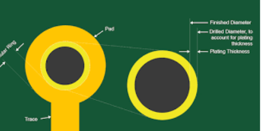
Vias are typically plated with copper to ensure electrical conductivity. However, leaving them open or unfilled can lead to several issues, which is why via filling is often employed.
2. Reasons for Filling and Plugging Vias
2.1 Preventing Solder Wicking and Short Circuits
One of the primary reasons for filling vias is to prevent solder from flowing into them during assembly—a phenomenon known as solder wicking. If vias are left open, solder can seep through, potentially causing:
- Short circuits if solder bridges adjacent vias or traces.
- Weak solder joints if solder intended for component leads is drawn away.
By filling vias with epoxy or conductive paste, manufacturers ensure that solder remains where it is needed, improving assembly reliability.
2.2 Enhancing Signal Integrity in High-Speed PCBs
In high-frequency and high-speed PCB designs, unfilled vias can act as stubs, causing signal reflections and impedance mismatches. These issues degrade signal quality, leading to:
- Increased insertion loss
- Signal distortion
- Electromagnetic interference (EMI)
Filling vias (especially with conductive materials) helps minimize stub effects, ensuring better signal transmission. Additionally, via-in-pad designs—where vias are placed directly under component pads—require filling to prevent solder voids and ensure a flat surface for component mounting.
2.3 Improving Thermal Management
Vias are often used for thermal dissipation, especially in power electronics and high-current applications. Filling vias with thermally conductive materials (such as copper or silver epoxy) enhances heat transfer from components to other PCB layers or heatsinks. This prevents overheating and improves long-term reliability.
2.4 Supporting High-Density Interconnect (HDI) PCBs
Modern electronics demand smaller and more densely packed PCBs. HDI (High-Density Interconnect) designs use microvias and stacked vias to maximize space efficiency. Filling these vias:
- Provides structural support, preventing collapse during lamination.
- Enables laser drilling for stacked and staggered microvias.
- Reduces the risk of air traps, which can cause delamination.
2.5 Preventing Contamination and Corrosion
Open vias can trap moisture, flux residues, and other contaminants during PCB fabrication and assembly. Over time, these contaminants may lead to:
- Corrosion of copper plating
- Electrical leakage
- Reduced insulation resistance
Filled vias seal these pathways, enhancing environmental resistance and long-term durability.
2.6 Facilitating Surface Mount Technology (SMT)
For via-in-pad applications—where vias are placed directly under component pads—filling is critical. Unfilled vias can cause:
- Solder drainage, leading to weak or incomplete joints.
- Uneven surfaces, making it difficult to place fine-pitch components like BGAs.
Filled and planarized vias provide a smooth surface, ensuring proper solder paste application and component placement.
3. Methods of Via Filling
3.1 Conductive Via Filling
- Copper Electroplating: Used for high-current and thermal vias.
- Silver Epoxy: Provides good conductivity and solderability.
- Conductive Pastes: Used in via-in-pad designs to ensure electrical continuity.
3.2 Non-Conductive Via Filling
- Epoxy Resins: Common for general-purpose via filling.
- Soldermask Plugging: Used to prevent solder wicking.
- Liquid Photoimageable (LPI) Materials: Provide precise filling for small vias.
3.3 Hybrid Approaches
Some designs use a combination of conductive and non-conductive fills, depending on the via’s function.
4. Applications of Filled Vias
- Consumer Electronics: Smartphones, tablets, and wearables use filled vias for miniaturization.
- Automotive Electronics: Improved reliability under harsh conditions.
- Aerospace and Defense: High-reliability PCBs with enhanced signal integrity.
- Medical Devices: Protection against moisture and contamination.
5. Challenges in Via Filling
While via filling offers many advantages, it also presents challenges:
- Increased manufacturing cost due to additional processing steps.
- Potential voids if filling is not done properly, leading to reliability issues.
- Material compatibility—some fillers may not withstand high-temperature reflow processes.
6. Conclusion
Filling and plugging vias in PCBs is a critical process that enhances reliability, signal integrity, thermal performance, and manufacturability. As electronic devices continue to shrink and demand higher performance, via filling techniques will become even more essential in PCB design and fabrication.
By understanding the reasons behind via filling—from preventing solder defects to enabling HDI designs—engineers can make informed decisions to optimize their PCB layouts for both functionality and durability.