
PCB and BOM Design for Manufacturability (DFM) Analysis
Abstract
Design for Manufacturability (DFM) is a critical aspect of printed circuit board (PCB) and Bill of Materials (BOM) development, ensuring that products can be efficiently and cost-effectively manufactured. This paper explores key considerations in PCB and BOM DFM analysis, including design guidelines, component selection, assembly processes, and testing methodologies. By optimizing designs for manufacturability, engineers can reduce production costs, improve yield rates, and accelerate time-to-market.
1. Introduction
The electronics manufacturing industry faces increasing pressure to deliver high-quality products at competitive prices while meeting tight deadlines. PCB and BOM DFM analysis plays a crucial role in bridging the gap between design and production, minimizing errors, and enhancing manufacturability. This paper examines best practices for PCB layout, component placement, material selection, and BOM optimization to ensure seamless manufacturing.
2. PCB Design for Manufacturability (DFM)
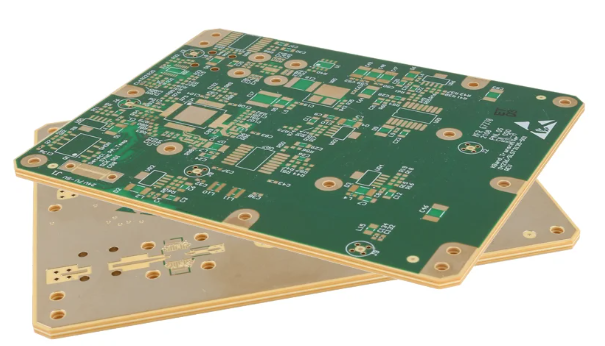
2.1. PCB Layout Considerations
A well-designed PCB layout is fundamental to manufacturability. Key factors include:
- Trace Width and Spacing: Adhering to manufacturer capabilities prevents short circuits and signal integrity issues.
- Via Placement: Minimizing unnecessary vias reduces drilling costs and improves reliability.
- Copper Balancing: Ensuring even copper distribution prevents warping during reflow soldering.
- Panelization: Efficient panel design maximizes material usage and assembly throughput.
2.2. Component Placement and Orientation
- Pick-and-Place Optimization: Components should be arranged to minimize robotic arm movement, reducing assembly time.
- Polarity and Silkscreen Markings: Clear markings prevent assembly errors.
- Thermal Management: High-power components should be spaced appropriately to avoid overheating.
2.3. Design Rule Checks (DRC) and DFM Software
Automated DFM tools (e.g., Altium, Cadence, Valor) validate designs against manufacturing constraints, identifying issues such as:
- Insufficient solder mask clearance
- Acid traps in copper traces
- Non-standard drill sizes
3. BOM Optimization for Manufacturability
3.1. Component Selection and Availability
- Preferred Parts: Using commonly stocked components reduces lead times.
- Alternative Sources: Identifying multiple suppliers mitigates supply chain risks.
- Lifecycle Management: Avoiding obsolete or end-of-life (EOL) parts prevents redesign delays.
3.2. Standardization and Simplification
- Reducing Unique Parts: Fewer part variants streamline inventory management.
- Common Footprints: Standardized footprints simplify assembly and testing.
3.3. Cost and Lead Time Analysis
- Value Engineering: Selecting cost-effective alternatives without compromising performance.
- Just-in-Time (JIT) Procurement: Balancing inventory costs with production needs.
4. Assembly Process Considerations
4.1. Surface Mount Technology (SMT) vs. Through-Hole
- SMT Advantages: Higher component density, faster assembly, and lower cost.
- Through-Hole Use Cases: Better mechanical strength for connectors and high-power components.
4.2. Soldering Techniques
- Reflow Soldering: Optimal for SMT components.
- Wave Soldering: Used for through-hole parts but requires careful thermal management.
- Selective Soldering: Combines benefits of reflow and wave soldering for mixed-technology boards.
4.3. Inspection and Testing
- Automated Optical Inspection (AOI): Detects soldering defects and misplaced components.
- In-Circuit Testing (ICT): Validates electrical functionality.
- Functional Testing: Ensures the final product meets specifications.
5. Common DFM Pitfalls and Solutions
5.1. Poorly Designed Pads and Stencils
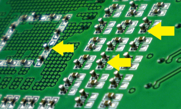
- Issue: Insufficient solder paste leads to weak joints.
- Solution: Follow IPC-7351 pad geometry standards.
5.2. Inadequate Thermal Relief
- Issue: Excessive heat dissipation causes soldering defects.
- Solution: Implement thermal relief connections in power planes.
5.3. Incorrect BOM Data
- Issue: Mismatched part numbers cause assembly errors.
- Solution: Cross-verify BOM entries with supplier datasheets.
6. Case Study: DFM Success Story
A consumer electronics company reduced PCB defects by 30% after implementing automated DFM checks and optimizing their BOM for preferred components. By collaborating with contract manufacturers early in the design phase, they achieved a 15% reduction in production costs.
7. Conclusion
Effective PCB and BOM DFM analysis is essential for reducing manufacturing defects, lowering costs, and improving product reliability. By integrating DFM principles early in the design process, engineers can enhance manufacturability and ensure smoother production cycles. Future advancements in AI-driven DFM tools will further streamline the transition from design to mass production.