
PCB Grounding Design Guidelines: Best Practices for Optimal Performance
Introduction
Printed Circuit Board (PCB) grounding is a critical aspect of electronic design that directly impacts signal integrity, electromagnetic compatibility (EMC), and overall system performance. Poor grounding can lead to noise coupling, ground loops, and increased electromagnetic interference (EMI), which can degrade circuit functionality. This article outlines essential PCB grounding design guidelines to ensure reliable and efficient circuit operation.
1. Understanding Grounding in PCBs
Grounding in PCBs refers to the method of providing a common reference point (ground plane) for all circuit components to ensure stable voltage levels and minimize noise. The primary objectives of grounding are:
- Signal Integrity (SI): Preventing signal distortion due to noise.
- Power Integrity (PI): Ensuring stable power distribution.
- EMI/EMC Control: Reducing electromagnetic interference and improving compatibility.
Grounding strategies vary depending on circuit complexity, frequency, and application requirements.
2. Types of Grounding Schemes
2.1 Single-Point Grounding
- Used in low-frequency circuits (<1 MHz).
- All ground connections meet at a single point to avoid ground loops.
- Suitable for analog circuits where noise sensitivity is high.
2.2 Multi-Point Grounding
- Used in high-frequency circuits (>10 MHz).
- Multiple ground connections reduce impedance and minimize ground bounce.
- Common in digital circuits and RF designs.
2.3 Hybrid Grounding
- Combines single-point and multi-point grounding.
- Uses capacitors or inductors to isolate different ground sections at different frequencies.
3. PCB Grounding Best Practices
3.1 Use a Solid Ground Plane
- A continuous copper plane provides the lowest impedance return path.
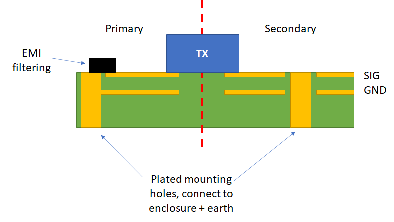
- Avoid splitting ground planes unless necessary (e.g., separating analog and digital grounds).
3.2 Separate Analog and Digital Grounds
- Analog circuits are sensitive to noise from digital switching.
- Use separate ground planes and connect them at a single point (star grounding).
3.3 Minimize Ground Loops
- Ground loops occur when multiple return paths create unwanted current flow.
- Use proper layout techniques to ensure a single return path for critical signals.
3.4 Proper Component Placement
- Place high-speed digital components close to the ground plane to reduce loop area.
- Group analog components together to minimize interference.
3.5 Via Placement for Ground Connections
- Use multiple vias to connect components to the ground plane, reducing inductance.
- Avoid long traces between components and ground connections.
3.6 Avoid Ground Plane Splits Under High-Speed Signals
- Splits can increase return path impedance and cause EMI issues.
- Ensure high-speed signals have an uninterrupted return path.
3.7 Use Decoupling Capacitors
- Place decoupling capacitors near IC power pins to provide a low-impedance path for high-frequency noise.
- Connect capacitors directly to the ground plane with short traces.
3.8 Implement Proper Power Plane Coupling
- Power and ground planes should be closely coupled to reduce noise.
- Use thin dielectric layers between power and ground planes for better capacitance.
3.9 Consider Split Grounds for Mixed-Signal PCBs
- If analog and digital circuits must coexist, use split grounds with a single connection point.
- Ensure signals do not cross split planes to avoid increased loop area.
3.10 Implement EMI Shielding Techniques
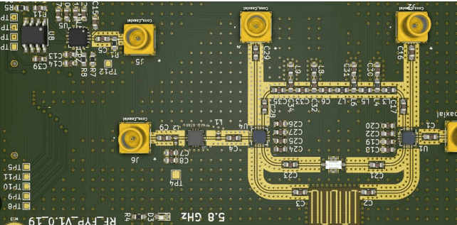
- Use guard rings or ground fences around sensitive traces.
- Apply ground stitching vias along PCB edges to reduce radiation.
4. Common Grounding Mistakes to Avoid
4.1 Floating Grounds
- Unconnected ground pins can cause unpredictable behavior.
- Always ensure all ground connections are properly tied to the ground plane.
4.2 Long Ground Traces
- Long traces increase inductance and impedance, degrading high-frequency performance.
- Use short, direct connections to the ground plane.
4.3 Ignoring Return Current Paths
- High-speed signals follow the path of least inductance, which is directly beneath the signal trace.
- Ensure the ground plane provides a clear return path.
4.4 Over-Splitting Ground Planes
- Excessive splits can lead to increased EMI and signal integrity issues.
- Only split grounds when absolutely necessary (e.g., isolating high-noise circuits).
4.5 Poor Via Usage
- Insufficient vias can create high-impedance ground connections.
- Use multiple vias for high-current paths and critical ground connections.
5. Advanced Grounding Techniques
5.1 Grounding in High-Speed PCBs
- Use buried or blind vias to reduce stub effects.
- Implement ground plane islands for RF shielding.
5.2 Grounding in Multi-Layer PCBs
- Dedicate entire layers to ground and power planes.
- Use symmetrical stack-ups to minimize warping and improve EMI performance.
5.3 Grounding for RF and Microwave PCBs
- Use coplanar waveguide grounding for controlled impedance.
- Implement via fences to suppress surface wave propagation.
6. Testing and Validation
After implementing grounding strategies, perform the following tests:
- Impedance Measurements: Ensure low-impedance ground paths.
- Signal Integrity Analysis: Check for reflections and crosstalk.
- EMI Testing: Verify compliance with EMC standards.
Conclusion
Proper PCB grounding design is essential for ensuring signal integrity, reducing noise, and achieving EMC compliance. By following these guidelines—using solid ground planes, separating analog and digital grounds, minimizing ground loops, and employing advanced techniques for high-speed designs—engineers can optimize PCB performance. Continuous testing and validation further ensure that grounding strategies are effective in real-world applications.
By adhering to these best practices, designers can avoid common pitfalls and create robust, high-performance PCBs for a wide range of applications.