
Design Considerations for Smart Bracelet PCB Boards
Introduction
The rapid advancement of wearable technology has led to the widespread adoption of smart bracelets, which monitor health metrics, track fitness activities, and provide notifications. At the heart of these devices lies the Printed Circuit Board (PCB), which integrates sensors, microcontrollers, wireless communication modules, and power management systems. Designing a PCB for a smart bracelet presents unique challenges due to size constraints, power efficiency requirements, and signal integrity concerns. This article explores key considerations in smart bracelet PCB design to ensure optimal performance, reliability, and manufacturability.
1. Size and Form Factor Constraints
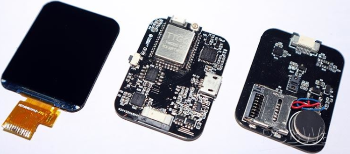
Smart bracelets are compact, requiring PCBs to be miniaturized while maintaining functionality. Key aspects include:
1.1. Flexible or Rigid-Flex PCBs
- Many smart bracelets use Flexible PCBs (FPCBs) or Rigid-Flex PCBs to conform to curved shapes.
- Flex PCBs reduce weight and improve durability but require careful handling during assembly.
1.2. Component Placement Optimization
- High-density interconnect (HDI) technology allows for smaller vias and tighter component placement.
- Critical components (MCU, sensors, antenna) should be positioned to minimize interference and maximize signal integrity.
1.3. Layer Stackup Considerations
- A 4-6 layer PCB is common, balancing complexity and cost.
- Dedicated layers for power and ground planes reduce noise and improve EMI performance.
2. Power Management and Battery Efficiency
Smart bracelets rely on small batteries, making power efficiency crucial.
2.1. Low-Power Components
- Select ultra-low-power MCUs (e.g., ARM Cortex-M series) and energy-efficient sensors.
- Use sleep modes to minimize power consumption during inactivity.
2.2. Power Distribution Network (PDN) Design
- Proper decoupling capacitors should be placed near ICs to stabilize voltage.
- Minimize voltage drops by using wider traces for high-current paths.
2.3. Battery Charging Circuitry
- Implement Li-ion/Polymer battery charging ICs with overcharge protection.
- Ensure proper thermal management to prevent overheating during charging.
3. Signal Integrity and EMI/EMC Considerations
Smart bracelets incorporate wireless communication (Bluetooth, NFC), requiring careful signal handling.
3.1. RF Antenna Design
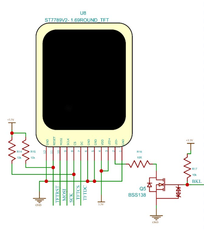
- Antenna placement is critical—keep it away from noisy components (motors, LCD drivers).
- Use a ground plane beneath the antenna to enhance radiation efficiency.
- Impedance matching (typically 50Ω for Bluetooth) minimizes signal reflection.
3.2. Shielding and Grounding
- Use shielded enclosures or copper pours to reduce EMI.
- Avoid ground loops by implementing a single-point grounding strategy.
3.3. High-Speed Signal Routing
- Route high-speed signals (USB, SPI, I2C) with controlled impedance.
- Keep traces short and avoid sharp angles to reduce signal degradation.
4. Sensor Integration and Noise Reduction
Smart bracelets include multiple sensors (accelerometer, heart rate, SpO2), requiring noise mitigation.
4.1. Proper Sensor Placement
- Keep analog sensors (PPG for heart rate) away from digital noise sources.
- Use guard rings or separate ground planes for sensitive analog circuits.
4.2. Filtering and Shielding
- Implement low-pass filters to eliminate high-frequency noise.
- Use ferrite beads to suppress high-frequency interference in power lines.
5. Thermal Management
Excessive heat can degrade performance and battery life.
5.1. Heat Dissipation Techniques
- Use thermal vias under high-power components (e.g., charging ICs).
- Avoid placing heat-sensitive components (battery, sensors) near heat sources.
5.2. Material Selection
- High-Tg (glass transition temperature) FR4 or polyimide substrates for flexible PCBs improve thermal stability.
6. Manufacturing and Reliability Considerations
Ensuring manufacturability and long-term reliability is essential.
6.1. Design for Manufacturing (DFM)
- Follow IPC standards for trace width, spacing, and via sizes.
- Avoid acid traps (acute angles in copper traces) that can cause etching issues.
6.2. Environmental Durability
- Apply conformal coating to protect against moisture and sweat.
- Use gold-plated contacts for charging pins to prevent corrosion.
6.3. Testing and Validation
- Perform Automated Optical Inspection (AOI) and functional testing post-assembly.
- Validate RF performance with antenna testing and EMI scans.
Conclusion
Designing a PCB for a smart bracelet involves balancing size constraints, power efficiency, signal integrity, and manufacturability. By carefully selecting components, optimizing layout, and adhering to best practices in RF and power management, engineers can create reliable and high-performance wearable devices. As smart bracelets evolve, advancements in flexible electronics and low-power design will further enhance their capabilities.
By addressing these key considerations, designers can ensure their smart bracelet PCBs meet the demands of modern wearable technology while maintaining robustness and efficiency.