
Function Principles and Application Characteristics of PCB Testing Instruments
Abstract
Printed Circuit Board (PCB) testing is a critical phase in electronics manufacturing, ensuring the reliability and functionality of PCBs before they are deployed in end products. PCB testing instruments employ various methodologies to detect defects, verify electrical continuity, and assess signal integrity. This paper explores the functional principles of PCB testing instruments, including in-circuit testing (ICT), flying probe testing, automated optical inspection (AOI), and boundary scan testing. Additionally, it discusses the application characteristics of these instruments, highlighting their advantages, limitations, and industry use cases.
1. Introduction
PCBs are the backbone of modern electronic devices, and their failure can lead to significant operational issues. To mitigate defects such as short circuits, open circuits, incorrect component placement, and soldering issues, PCB testing instruments are employed at different stages of production. These instruments vary in complexity, speed, and accuracy, depending on the testing requirements.
This paper examines the key functional principles of PCB testing instruments and their application characteristics in electronics manufacturing.
2. Functional Principles of PCB Testing Instruments
2.1 In-Circuit Testing (ICT)
Principle:
ICT is a robust testing method that verifies the electrical performance of individual components on a PCB. It uses a bed-of-nails fixture that makes contact with test points on the board, applying voltage and current to measure resistance, capacitance, and other parameters.
Key Features:
- High fault coverage for manufacturing defects.
- Tests components in their powered (live) or unpowered state.
- Detects opens, shorts, missing components, and incorrect values.
Limitations:
- Requires custom fixtures, increasing setup costs.
- Less effective for high-frequency signal testing.
2.2 Flying Probe Testing
Principle:
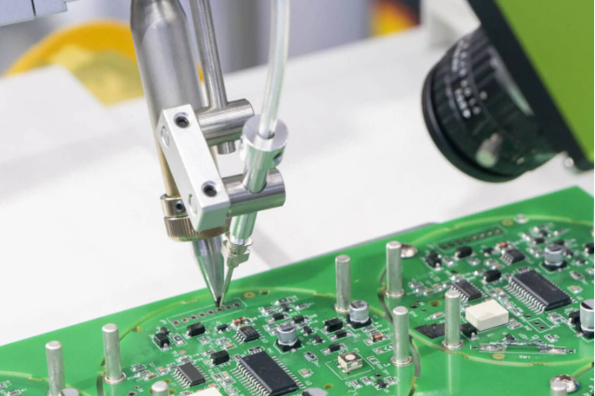
Flying probe testers use movable probes to access test points on a PCB without requiring a fixed fixture. They perform continuity checks, component verification, and basic functional testing.
Key Features:
- No need for custom fixtures, reducing cost for low-volume production.
- Flexible and programmable for different PCB designs.
- Suitable for prototype and small-batch testing.
Limitations:
- Slower than ICT due to mechanical probe movement.
- Limited in high-power and high-frequency testing.
2.3 Automated Optical Inspection (AOI)
Principle:
AOI systems use high-resolution cameras and image processing algorithms to inspect PCBs for soldering defects, component misalignment, and surface anomalies.
Key Features:
- Non-contact testing, preventing mechanical damage.
- Fast inspection suitable for high-volume production.
- Detects visual defects such as solder bridges and missing components.
Limitations:
- Cannot test electrical functionality.
- May produce false positives due to lighting or angle variations.
2.4 Boundary Scan Testing (IEEE 1149.1)
Principle:
Boundary scan testing uses integrated test circuitry (JTAG) embedded in ICs to verify interconnections and functional logic without physical probes.
Key Features:
- Effective for complex, high-density PCBs.
- Tests inaccessible nodes without physical probes.
- Supports debugging and programming of onboard chips.
Limitations:
- Requires JTAG-compliant components.
- Limited in analog and power circuit testing.
3. Application Characteristics of PCB Testing Instruments
3.1 Manufacturing Testing
PCB testing instruments are widely used in electronics manufacturing to ensure quality control. ICT and AOI are commonly deployed in mass production, while flying probe testers are preferred for prototypes.
3.2 Functional Validation
Beyond structural defects, functional testers validate the operational behavior of PCBs under real-world conditions, including power-up sequences and signal integrity checks.
3.3 Repair and Rework
Testing instruments help identify faulty components, enabling efficient repair processes. Boundary scan testing is particularly useful for diagnosing complex digital circuits.
3.4 Industry-Specific Applications
- Consumer Electronics: High-speed AOI and ICT for smartphones and laptops.
- Automotive: Rigorous environmental and functional testing for reliability.
- Aerospace and Defense: High-reliability boundary scan and flying probe testing.
4. Conclusion
PCB testing instruments play a vital role in ensuring the quality and reliability of electronic assemblies. Each testing method—ICT, flying probe, AOI, and boundary scan—has distinct functional principles and application characteristics. The choice of testing instrument depends on factors such as production volume, PCB complexity, and cost considerations.
As PCB technology evolves with higher component density and advanced materials, testing methodologies must also advance to meet new challenges. Future trends include AI-driven optical inspection, enhanced boundary scan techniques, and integrated testing solutions for IoT and 5G applications