
How to Set Solder Mask Over Vias in Various PCB Design Software
Introduction
Solder mask over vias (commonly referred to as “via tenting” or “via capping”) is a crucial PCB manufacturing consideration that affects both the aesthetics and functionality of printed circuit boards. This process involves covering vias with solder mask to protect them from environmental factors, prevent solder wicking during assembly, and improve surface planarity for fine-pitch components. This comprehensive guide will explore how to properly configure via tenting in major PCB design software packages.
Understanding Via Tenting Options
Before diving into software-specific settings, it’s important to understand the different via tenting options available:
- Full tenting: Complete coverage of the via with solder mask on both sides
- Partial tenting: Solder mask covers only one side of the via
- Tenting with openings: Small openings in the solder mask over the via
- Plugged vias: Vias filled with epoxy or conductive material before solder mask application
- Capped vias: Similar to plugged vias but with a planar surface
Each option serves different purposes in PCB manufacturing and assembly processes.
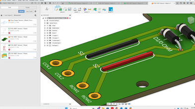
Altium Designer Via Tenting Configuration
Setting Via Tenting Properties
- Accessing via properties:
- Right-click on a via and select “Properties”
- Alternatively, use the PCB panel to select multiple vias
- Tenting options:
- Check “Tented” for full tenting on top and/or bottom layers
- Use “Force complete tenting on top/bottom” for strict enforcement
- Design Rule Check (DRC):
- Navigate to Design > Rules > Manufacturing > Solder Mask Expansion
- Set negative expansion values for proper tenting
- Batch processing:
- Use the “Find Similar Objects” feature to apply tenting to multiple vias
- Create via templates with predefined tenting properties
Output Generation Considerations
When generating Gerber files:
- Ensure solder mask layers (typically .GTS and .GBS) include the tented vias
- Verify that tenting settings are properly reflected in the Gerber preview
- Check the solder mask expansion values in the output job file
Cadence Allegro Via Tenting Setup
Via Tenting in Constraint Manager
- Access the Constraint Manager:
- Select Setup > Constraints > Constraint Manager
- Set physical constraints:
- Navigate to Physical > Via > SolderMask_Top/SolderMask_Bottom
- Define the solder mask expansion values (negative for tenting)
- Via styles:
- Create or modify via styles to include tenting properties
- Assign these styles to specific via instances or nets
Implementing Via Tenting
- Individual via properties:
- Right-click a via and select “Edit Properties”
- Set SOLDERMASK_TOP/BOTTOM to “Tented”
- Batch modifications:
- Use the “Edit > Properties” menu to change multiple vias
- Apply filters to select specific via types or sizes
- Manufacturing checks:
- Run DRC to verify tenting compliance
- Use the solder mask viewer to visualize tented vias
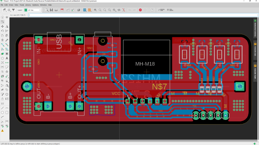
KiCad Via Tenting Configuration
Setting Up Via Tenting
- Via properties dialog:
- Double-click on a via to access properties
- Check “Tented” under solder mask settings
- Global settings:
- Access Preferences > PCB Editor > Defaults
- Set default via properties including tenting
- Design rules:
- Open File > Board Setup > Solder Mask/Paste
- Adjust solder mask clearance values for vias
Export Considerations
- Gerber generation:
- Use File > Fabrication Outputs > Gerbers
- Ensure “Exclude PCB edge layer from other layers” is unchecked
- Verify tented vias appear correctly in Gerber preview
- Interactive HTML BOM:
- Include tenting information in the BOM for manufacturing clarity
Eagle (Autodesk) Via Tenting Setup
Configuring Via Tenting
- Via parameters:
- Use the “Change” tool and select a via
- Set “Stop” parameter to “Yes” for tenting
- Design rules:
- Access Edit > Design Rules > Mask
- Set “Stop” expansion to negative values for tenting
- ULP scripts:
- Utilize User Language Programs for batch tenting operations
- Create scripts to automate via tenting based on size or location
Output Verification
- CAM processor:
- Configure solder mask layers in the CAM job
- Verify tenting settings in the layer configuration
- DRC settings:
- Run electrical rule checks to ensure tenting doesn’t violate clearances
- Adjust tenting parameters if conflicts arise
OrCAD PCB Designer Via Tenting
Implementing Via Tenting
- Via properties:
- Right-click a via and select “Properties”
- Set SOLDERMASK_TOP/BOTTOM to “Full” for tenting
- Constraint management:
- Use Constraint Manager to define tenting rules
- Apply rules to specific net classes or via types
- Cross-section editor:
- Define via structures with built-in tenting properties
- Apply these structures throughout the design
Manufacturing Outputs
- Gerber settings:
- Configure negative solder mask expansions in the artwork control form
- Verify tenting in the Gerber preview
- IPC-356 netlist:
- Include tenting information for manufacturing reference
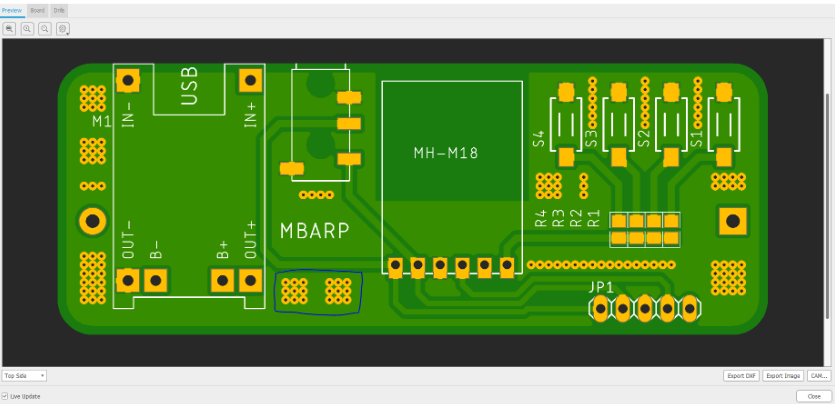
PADS Via Tenting Configuration
Setting Up Via Tenting
- Via properties:
- Select a via and access its properties
- Enable “Tented Top” and/or “Tented Bottom” options
- Design rules:
- Setup > Design Rules > Default > Solder Mask
- Set appropriate expansion values for tenting
- Batch processing:
- Use the “Filter” to select multiple vias
- Apply tenting properties to the selection
Output Generation
- CAM documentation:
- Configure solder mask layers in the CAM setup
- Verify tenting appears correctly in the preview
- Manufacturing notes:
- Clearly specify tenting requirements in fabrication drawings
General Best Practices for Via Tenting
Design Considerations
- Via size and spacing:
- Smaller vias are easier to tent reliably
- Maintain proper spacing between tented vias and components
- Manufacturing capabilities:
- Consult with your PCB fabricator about their tenting capabilities
- Understand minimum via size for reliable tenting
- Testing requirements:
- Leave critical test points untented for probing
- Consider partial tenting for vias needing electrical access
Software-Specific Tips
- Template creation:
- Develop via templates with predefined tenting settings
- Share templates across design teams for consistency
- Design rule checks:
- Implement DRC rules to flag untented vias
- Create custom checks for via tenting compliance
- Version control:
- Document tenting requirements in design specifications
- Track changes to tenting settings across revisions
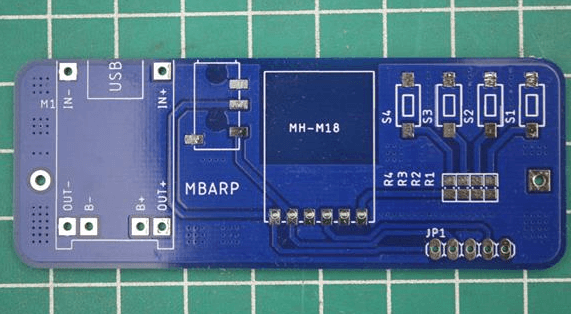
Troubleshooting Common Via Tenting Issues
Software-Related Problems
- Tenting not reflected in outputs:
- Verify Gerber generation settings
- Check for conflicting design rules
- Inconsistent tenting application:
- Review via properties for exceptions
- Check for inherited properties from templates
- DRC errors with tenting:
- Adjust clearance rules for tented vias
- Consider creating specific tenting design rules
Manufacturing Considerations
- Tenting failures:
- Ensure via sizes are within manufacturer capabilities
- Consider via fill options for better tenting reliability
- Solder mask alignment:
- Account for registration tolerances in your design
- Specify critical areas where tenting must be precise
- Communication with fabricators:
- Clearly mark tenting requirements in fabrication notes
- Provide sample files showing expected tenting results
Advanced Via Tenting Techniques
Selective Tenting
- Component-specific tenting:
- Tent vias under BGA components for better planarity
- Leave vias in test areas untented
- Layer-specific tenting:
- Tent only one side of vias in specific areas
- Use partial tenting for vias requiring limited protection
High-Density Designs
- Microvia tenting:
- Special considerations for HDI designs
- Laser-drilled via tenting parameters
- Via-in-pad configurations:
- Tenting versus filling decisions
- Planarization requirements for fine-pitch components
Conclusion
Proper configuration of via tenting in PCB design software requires understanding both the software capabilities and manufacturing requirements. Each EDA tool approaches via tenting differently, but the fundamental goal remains the same: to clearly communicate your design intent to the PCB manufacturer. By following the software-specific guidelines outlined in this article and maintaining clear communication with your fabrication partners, you can ensure reliable via tenting implementation in your PCB designs.
Remember that while software settings are important, they must align with your manufacturer’s capabilities. Always verify tenting requirements with your fabrication house and consider requesting test coupons for new via tenting configurations. With careful attention to these details, you can achieve optimal results in your PCB designs while leveraging the protective and aesthetic benefits of proper via tenting implementation.
.