
Electrostatic Discharge (ESD) Protection Methods in PCB Design
Introduction
Electrostatic discharge (ESD) is a sudden flow of electricity between two electrically charged objects, which can cause severe damage to electronic components. In printed circuit board (PCB) design, ESD protection is critical to ensuring the reliability and longevity of electronic devices. Without proper safeguards, ESD can lead to catastrophic failures, latent defects, or reduced performance in sensitive circuits.
This article explores various ESD protection methods in PCB design, including layout strategies, component selection, grounding techniques, and shielding approaches. By implementing these methods, designers can mitigate ESD risks and enhance the robustness of their electronic systems.
1. Understanding ESD and Its Impact on PCBs
1.1 What is ESD?
Electrostatic discharge occurs when a high-voltage charge is transferred between objects with different potentials. Common sources of ESD include:
- Human handling (e.g., touching components without grounding)
- Friction between insulating materials
- Improper handling of PCBs during manufacturing and assembly
1.2 Effects of ESD on PCBs
- Immediate Failure: High-voltage ESD can instantly destroy semiconductor devices (e.g., ICs, transistors).
- Latent Damage: Weak ESD events may degrade components over time, leading to intermittent failures.
- Signal Integrity Issues: ESD-induced noise can disrupt high-speed signals, causing data corruption.
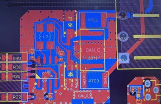
2. Key ESD Protection Methods in PCB Design
To safeguard PCBs against ESD, designers must adopt a multi-layered approach, including proper layout techniques, component selection, and grounding strategies.
2.1 PCB Layout Strategies for ESD Protection
A. Proper Grounding Techniques
- Single-Point Grounding: Ensures all ground connections meet at a single low-impedance point, minimizing ground loops.
- Ground Planes: Using solid ground planes reduces impedance and provides a stable reference for ESD currents.
- Partitioning Grounds: Separating analog, digital, and power grounds prevents noise coupling.
B. Trace Routing Considerations
- Minimize Loop Areas: Large loops act as antennas for ESD-induced noise; keep high-speed traces short and direct.
- Avoid Sharp Corners: Use 45° or curved traces to reduce charge accumulation.
- Increase Trace Spacing: Wider spacing between traces reduces capacitive coupling from ESD events.
C. Shielding and Isolation
- Faraday Cages: Enclosing sensitive components in conductive shields (e.g., metal cans) blocks ESD interference.
- Guard Rings: Placing grounded copper rings around high-impedance nodes diverts ESD currents away from critical traces.
2.2 ESD Protection Components
A. Transient Voltage Suppressors (TVS Diodes)
- TVS diodes clamp ESD voltages to safe levels by diverting excess current to ground.
- Placed near connectors and I/O ports for optimal protection.
B. Varistors (MOVs – Metal Oxide Varistors)
- Varistors absorb high-voltage spikes and are commonly used in power supply lines.
C. ESD Suppression Filters
- RC filters and ferrite beads reduce high-frequency noise from ESD events.
D. Spark Gaps
- Spark gaps provide a low-resistance path for ESD currents in high-voltage applications.
2.3 Enclosure and System-Level ESD Protection
- Conductive Housings: Metallic or conductive-coated enclosures dissipate ESD charges.
- ESD-Safe Connectors: Shielded connectors prevent ESD from entering through cables.
- Proper PCB Mounting: Ensuring PCBs are securely grounded to the chassis prevents floating potentials.
3. Testing and Compliance with ESD Standards
3.1 Common ESD Standards
- IEC 61000-4-2: Defines ESD immunity testing for electronic equipment.
- ANSI/ESD S20.20: Establishes ESD control programs for manufacturing.
- MIL-STD-883: Military standard for ESD testing of microelectronics.
3.2 ESD Testing Methods
- Human Body Model (HBM): Simulates ESD from human contact (e.g., ±2kV to ±15kV).
- Machine Model (MM): Represents ESD from automated equipment.
- Charged Device Model (CDM): Tests ESD susceptibility of packaged ICs.
.
4. Best Practices for ESD-Safe PCB Assembly
- Use Anti-Static Workstations: Conductive mats and wrist straps prevent charge buildup.
- ESD-Safe Packaging: Store and transport PCBs in shielded bags.
- Humidity Control: Maintain 40-60% relative humidity to reduce static accumulation.
5. Case Study: ESD Protection in High-Speed PCB Design
A high-speed communication PCB was experiencing intermittent failures due to ESD. The following improvements were made:
- Added TVS diodes near Ethernet and USB ports.
- Implemented a multilayer ground plane for better current dissipation.
- Used guard traces around sensitive RF components.
After these changes, the PCB passed IEC 61000-4-2 Level 4 (±8kV contact, ±15kV air discharge) testing.
6. Conclusion
ESD protection is a critical aspect of PCB design, requiring a combination of layout optimization, component selection, and system-level shielding. By following industry best practices and adhering to ESD standards, designers can ensure robust and reliable electronic products.