
PCB Layout and Routing Requirements for Reset Circuits
Introduction
Reset circuits are among the most critical yet often overlooked components in electronic system design. These circuits ensure proper initialization of digital systems by generating a clean, stable reset signal during power-up, power-down, and brownout conditions. While the schematic design of reset circuits receives considerable attention, the PCB implementation is equally important and frequently the source of system reliability issues. This article details the essential PCB layout and routing requirements for reset circuits to ensure robust system operation.
Fundamental Characteristics of Reset Circuits
Reset circuits typically consist of:
- A reset generator IC or RC network
- Possible debouncing components
- Voltage monitoring components (for power-on reset)
- Optional manual reset switches
These circuits share several common characteristics that influence their PCB implementation:
- High impedance nodes: Many reset circuits contain high impedance points susceptible to noise coupling
- Timing sensitivity: Reset pulse width must meet minimum requirements for proper processor initialization
- Noise sensitivity: Glitches on reset lines can cause unintended system resets
- Critical timing relationship: Must maintain proper timing relative to clock signals and power supply stabilization
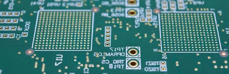
PCB Layout Guidelines for Reset Circuits
1. Component Placement
Priority placement:
- Place reset circuit components close to the device being reset (typically within 1-2 cm of the microcontroller)
- Position reset generators near the power supply they’re monitoring
Placement hierarchy:
- Reset generator IC or RC network
- Decoupling capacitors
- Manual reset switch (if present)
- Any filtering components
Special considerations:
- For multi-voltage systems, place voltage monitor ICs near the power supply they’re monitoring
- Keep reset circuits away from:
- High-frequency clock signals
- Switching power supplies
- High-current traces
- Electromechanical components
2. Power Supply Decoupling
Proper decoupling is essential for reliable reset circuit operation:
- Use a 0.1μF ceramic capacitor placed within 5mm of the reset IC’s VCC pin
- For systems with potential power transients, add a 1-10μF tantalum or electrolytic capacitor
- Ensure low-impedance connection to ground plane
3. Grounding Considerations
- Provide a solid ground connection for reset circuits
- Avoid sharing ground vias with high-current devices
- For mixed-signal systems, connect reset circuit grounds to the digital ground plane
- Maintain continuous ground plane beneath reset circuits
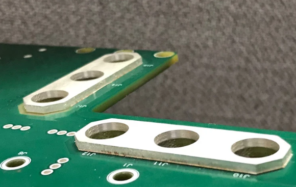
PCB Routing Requirements
1. Reset Signal Routing
Trace geometry:
- Minimum width: 0.2mm (8mil), preferred: 0.25-0.3mm (10-12mil)
- Avoid 90° angles; use 45° angles or curves
- Maintain consistent impedance along the entire path
Routing priority:
- Route reset signals before other signals in the layout process
- Give reset signals higher priority than general I/O signals
Length control:
- Keep reset traces as short as possible (typically <5cm)
- For distributed systems, consider using separate reset generators rather than long traces
2. Crosstalk Prevention
- Maintain minimum 3X trace width spacing from adjacent signals
- For parallel runs longer than 2.5cm, increase spacing to 5X trace width
- Route reset signals adjacent to ground traces or ground planes when possible
- Avoid routing reset signals parallel to:
- Clock signals
- High-speed data lines
- Switching power supply traces
3. Layer Stackup Considerations
- Preferred layer: Adjacent to solid ground plane
- Avoid routing reset signals on outer layers when possible
- If outer layer routing is necessary, provide ground flood on both sides
- For multi-layer boards, route reset signals on layers between ground planes
4. Via Usage
- Minimize via count in reset traces (ideally zero)
- If vias are necessary:
- Use one via per layer transition
- Place return vias nearby for ground continuity
- Avoid sharing vias with other signals
- Size vias appropriately for current carrying capacity (typically 0.3mm drill/0.6mm pad)

Special Cases and Advanced Techniques
1. Multi-Processor Systems
For systems with multiple devices requiring reset:
Centralized reset:
- Use star topology routing from reset generator
- Maintain equal trace lengths to all devices when possible
- Consider buffer ICs for fan-out >4
Distributed reset:
- Place local reset generators near each major IC
- Synchronize reset timing through proper component selection
2. Manual Reset Switches
- Use debounced switches (hardware or software)
- Route switch traces with additional clearance (minimum 5mm from other signals)
- Include TVS diodes for ESD protection in accessible switches
- Implement proper pull-up/pull-down resistors close to the switch
3. High-Reliability Systems
For mission-critical applications:
- Implement redundant reset circuits
- Use guard rings around sensitive reset components
- Consider conformal coating for environmental protection
- Implement test points for reset signal verification
4. High-Speed Design Considerations
For systems with fast edge rates:
- Terminate reset lines if length exceeds λ/10 of the harmonic content
- Use series termination resistors (typically 22-100Ω) near the driver
- Match impedance to prevent reflections
- Simulate reset signal integrity in high-speed designs
Verification and Testing
After implementing the PCB layout:
- Visual inspection:
- Verify reset trace routing and clearance
- Check component placement proximity
- Confirm decoupling capacitor placement
- Electrical testing:
- Measure reset pulse width under various conditions
- Verify noise immunity with oscilloscope
- Test reset timing relative to power supply stabilization
- Environmental testing:
- Perform power cycling tests
- Conduct EMC/EMI testing
- Verify operation under temperature extremes
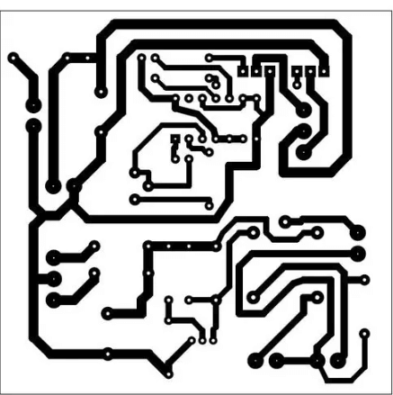
Common Pitfalls and Solutions
Problem: Intermittent resets during operation
Solution: Improve noise immunity through better routing, additional filtering, or Schmitt trigger inputs
Problem: Failure to reset during power-up
Solution: Verify reset timing matches processor requirements, adjust RC time constant if needed
Problem: Reset signal ringing
Solution: Add series termination, reduce trace length, or implement proper impedance matching
Problem: ESD susceptibility
Solution: Add TVS diodes, implement proper grounding, increase clearance around accessible reset components
Conclusion
Proper PCB layout and routing of reset circuits is essential for system reliability. By following these guidelines—careful component placement, controlled impedance routing, proper grounding, and noise reduction techniques—designers can ensure robust reset operation under all conditions. Remember that while reset circuits may seem simple, their implementation requires careful attention to detail to prevent subtle system failures that can be difficult to diagnose. Always verify reset circuit operation across all expected operating conditions and environmental factors to guarantee reliable system performance.