
Challenges in Rapid Prototyping of Multi-layer PCB Boards
Introduction
The rapid prototyping of multi-layer Printed Circuit Boards (PCBs) is a critical process in the electronics industry, enabling designers and engineers to quickly test and validate their designs before mass production. However, the process of creating multi-layer PCBs in a short timeframe presents numerous technical and logistical challenges. These challenges range from design complexity and material selection to manufacturing precision and quality control.
This article explores the key difficulties encountered in the rapid prototyping of multi-layer PCBs, including:
- Design Complexity and Signal Integrity
- Material Selection and Thermal Management
- Manufacturing Precision and Layer Alignment
- Via Processing and Interconnect Reliability
- Time Constraints and Cost Efficiency
- Testing and Quality Assurance
Understanding these challenges is essential for optimizing the rapid prototyping process and ensuring high-quality, functional PCBs.
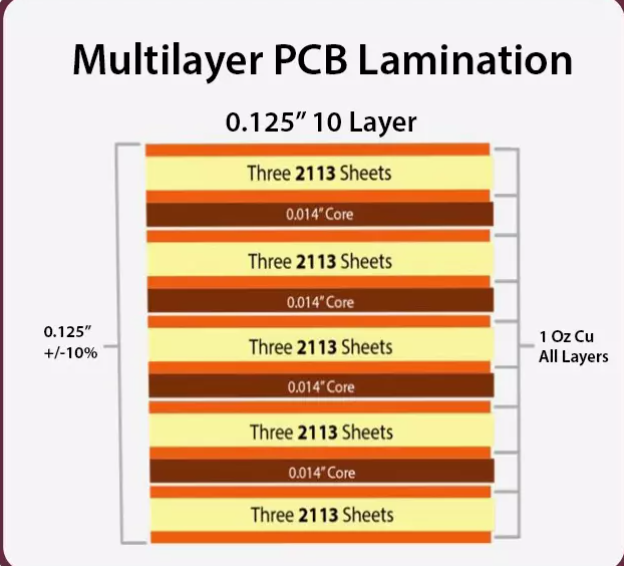
1. Design Complexity and Signal Integrity
Multi-layer PCBs (typically 4+ layers) are significantly more complex than single or double-layer boards due to their intricate routing and signal distribution requirements. Some of the primary challenges include:
a. High-Speed Signal Routing
- Multi-layer PCBs often handle high-frequency signals, requiring careful impedance control to prevent signal degradation.
- Crosstalk between adjacent layers can lead to electromagnetic interference (EMI), necessitating proper shielding and ground plane design.
b. Power and Ground Plane Distribution
- Ensuring stable power delivery across multiple layers requires well-designed power planes and decoupling capacitors.
- Poor power distribution can lead to voltage drops and noise, affecting circuit performance.
c. Design Rule Checks (DRC) and DFM Considerations
- Rapid prototyping demands quick design iterations, but complex multi-layer layouts must still comply with Design for Manufacturing (DFM) rules.
- Errors in spacing, trace width, or via placement can lead to fabrication failures.
2. Material Selection and Thermal Management
The choice of materials significantly impacts the performance and reliability of multi-layer PCBs, especially in rapid prototyping where time constraints limit extensive testing.
a. Dielectric Materials and Layer Stackup
- High-frequency applications require low-loss dielectric materials (e.g., Rogers, FR-4 High-Tg).
- Incorrect material selection can lead to signal loss or thermal expansion issues.
b. Thermal Dissipation Challenges
- Multi-layer boards generate more heat due to increased component density.
- Poor thermal management can cause delamination or solder joint failures.
c. Coefficient of Thermal Expansion (CTE) Mismatch
- Different materials expand at different rates when heated, leading to mechanical stress.
- This is particularly problematic in high-reliability applications (e.g., aerospace, automotive).
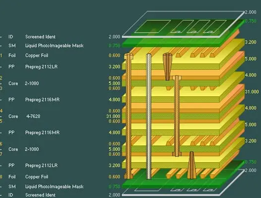
3. Manufacturing Precision and Layer Alignment
Achieving precise alignment between layers is crucial for multi-layer PCBs, but rapid prototyping introduces several challenges:
a. Registration Accuracy
- Misalignment between layers can cause short circuits or open connections.
- Advanced laser drilling and optical alignment systems are required but increase costs.
b. Lamination Process Control
- Uneven pressure or temperature during lamination can lead to voids or delamination.
- Rapid prototyping often uses faster curing resins, which may affect bond strength.
c. Copper Thickness and Etching Uniformity
- Inconsistent copper plating can lead to impedance mismatches.
- Over-etching or under-etching affects trace integrity.
4. Via Processing and Interconnect Reliability
Vias (plated through-holes, blind/buried vias) are essential for inter-layer connections but present challenges in rapid prototyping:
a. Microvia Drilling and Plating
- Laser drilling for HDI (High-Density Interconnect) PCBs requires high precision.
- Incomplete via plating can lead to poor conductivity or reliability issues.
b. Via Filling and Reliability
- Filled vias improve thermal and electrical performance but require additional process steps.
- Rapid curing via fill materials may introduce voids or cracks.
c. Thermal Stress on Vias
- Repeated thermal cycling (e.g., in power electronics) can cause via barrel cracking.
- Requires careful material selection and process control.
5. Time Constraints and Cost Efficiency
Rapid prototyping aims to reduce lead times, but this can introduce trade-offs:
a. Expedited Fabrication vs. Quality
- Faster production may skip some quality checks, increasing failure risks.
- Balancing speed with reliability is a key challenge.
b. High Setup Costs for Small Batches
- Prototyping small quantities is cost-inefficient due to setup and tooling expenses.
- Some manufacturers impose minimum order quantities (MOQs).
c. Supply Chain and Material Availability
- Short lead times require readily available materials, limiting options.
- Specialty materials (e.g., high-frequency laminates) may have long lead times.
6. Testing and Quality Assurance
Ensuring functionality in a short timeframe is difficult due to:
a. Limited Time for Extensive Testing
- Rapid prototypes may undergo only basic electrical testing, missing latent defects.
- Automated Optical Inspection (AOI) and X-ray inspection add time and cost.
b. Signal Integrity Validation
- High-speed designs require time-domain reflectometry (TDR) or network analysis, which are time-consuming.
c. Reliability Testing (Thermal, Mechanical)
- Accelerated life testing is often skipped in rapid prototyping, risking field failures.
Conclusion
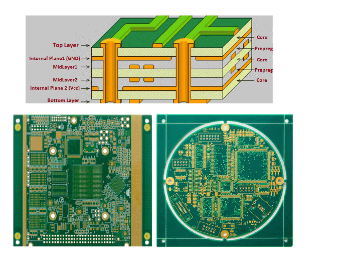
Rapid prototyping of multi-layer PCBs is essential for modern electronics development but comes with significant challenges. Design complexity, material selection, manufacturing precision, via reliability, time constraints, and testing limitations all contribute to the difficulty of producing high-quality prototypes quickly.
To overcome these challenges, engineers must leverage advanced design tools, collaborate closely with fabrication partners, and adopt emerging technologies like additive manufacturing and AI-assisted DFM checks. By addressing these issues, the industry can continue to accelerate innovation while maintaining high standards of PCB performance and reliability.