Why is it Essential to Keep PCBs Clean?
Introduction
Printed Circuit Boards (PCBs) form the backbone of modern electronics, found in everything from smartphones and computers to medical devices and aerospace systems. As electronic components become smaller and more densely packed, the importance of maintaining PCB cleanliness has grown exponentially. Cleanliness in PCBs isn’t merely about aesthetics; it’s a critical factor that affects performance, reliability, and longevity of electronic devices. This article explores the multifaceted reasons why keeping PCBs clean is essential, examining the technical, operational, and economic implications of PCB contamination.
The Nature of PCB Contamination
PCB contamination can originate from various sources throughout the manufacturing process and during the product’s operational life. Common contaminants include:
- Flux residues from soldering processes
- Dust and particulate matter from the environment
- Metallic dendrites formed by electrochemical migration
- Oils and greases from human handling
- Moisture and ionic contaminants that promote corrosion
- Mold release agents from plastic components
These contaminants can be conductive, corrosive, or both, creating multiple pathways for circuit failure. Even seemingly benign substances like fingerprint oils can become problematic under certain conditions.
Electrical Performance and Signal Integrity
Clean PCBs are fundamental to maintaining optimal electrical performance. Contaminants can significantly impact a board’s electrical characteristics in several ways:
- Leakage Currents: Ionic contamination on PCB surfaces can create unintended current paths between conductors, leading to leakage currents that disrupt circuit operation. These parasitic currents can cause signal distortion, particularly in high-impedance circuits where even nanoampere-level leakage can be problematic.
- Dielectric Properties: Contaminants can alter the dielectric properties of the PCB substrate, affecting impedance matching in high-frequency circuits. This is particularly critical in RF and microwave applications where consistent dielectric properties are essential for signal integrity.
- Surface Insulation Resistance (SIR): Conductive contaminants dramatically reduce SIR, potentially leading to short circuits or altered circuit behavior. Many industry standards (such as IPC-A-610) specify minimum SIR requirements that can only be met with properly cleaned PCBs.
- High Voltage Breakdown: In high-voltage applications, contaminants can create preferential paths for arcing, significantly reducing the board’s dielectric strength. Even non-conductive contaminants can trap moisture or particulates that facilitate breakdown.
Reliability and Long-Term Performance
The long-term reliability of electronic assemblies heavily depends on PCB cleanliness. Contamination contributes to several failure mechanisms:
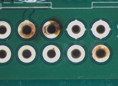
- Electrochemical Migration: Ionic contaminants in the presence of moisture can lead to dendritic growth between conductors. These metallic dendrites, typically composed of tin, lead, or silver, can eventually bridge gaps between traces, causing short circuits. This phenomenon is particularly prevalent in humid environments and is a leading cause of field failures in contaminated assemblies.
- Corrosion: Many contaminants act as electrolytes that accelerate corrosion of metal traces and components. Chlorides, sulfates, and other ionic species promote oxidation of copper traces and component leads, leading to increased resistance and eventual open circuits. Corrosion is an insidious process that may take months or years to manifest, often after the product has been deployed in the field.
- Conductive Anodic Filament (CAF) Formation: A particularly destructive failure mechanism where copper migrates through the glass fibers in the PCB laminate, creating conductive paths between adjacent vias or traces. Moisture and ionic contamination significantly accelerate CAF formation.
- Intermetallic Growth: Contaminants at solder joints can interfere with proper intermetallic formation, creating weak bonds that fail under thermal or mechanical stress. These defects often appear as intermittent failures that are difficult to diagnose.
Manufacturing and Process Considerations
PCB cleanliness affects not only the final product but also the manufacturing process itself:
- Soldering Defects: Contaminants on pads or components can lead to poor solder wetting, resulting in weak joints, voids, or complete non-wetting. Flux residues left from previous processes can interfere with subsequent soldering operations.
- Conformal Coating Adhesion: Most conformal coatings require clean surfaces for proper adhesion. Contaminants create weak boundaries where moisture can penetrate, undermining the coating’s protective function. IPC standards typically specify that surfaces must be clean to within 3.5 µg/cm² of ionic contamination for reliable coating adhesion.
- Automated Optical Inspection (AOI): Contaminants can obscure features or create false indications during automated inspection, leading to unnecessary rework or missed defects.
- Testing and Probing: Contamination at test points can increase contact resistance during in-circuit testing, producing false failures and increasing test time and rework costs.
Industry Standards and Requirements
Various industry standards underscore the importance of PCB cleanliness:
- IPC-J-STD-001: Requires that “solder joints shall be free of flux residues that could interfere with visual inspection, testing, or the operation of the product.”
- IPC-A-610: Establishes cleanliness requirements for different product classes, with Class 3 (high-reliability) products having the most stringent requirements.
- IPC-TM-650: Provides test methods for measuring ionic contamination, typically requiring less than 1.56 µg/cm² of NaCl equivalence for most high-reliability applications.
- MIL-STD-2000: Military standards often require exhaustive cleaning processes and verification testing to ensure long-term reliability in harsh environments.
Non-compliance with these standards can lead to product failures, warranty claims, and in some industries (medical, aerospace, automotive), potential liability issues.
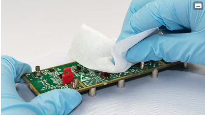
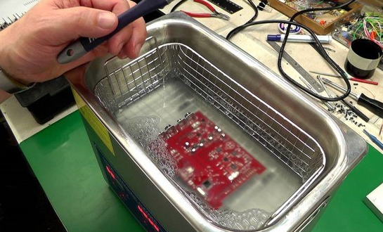
Cleaning Methods and Technologies
Maintaining PCB cleanliness requires appropriate cleaning processes:
- Aqueous Cleaning: Uses water with added saponifiers to remove ionic contaminants. Effective for most fluxes but requires proper drying.
- Solvent Cleaning: Uses hydrocarbon or fluorinated solvents to remove non-polar contaminants like oils and greases.
- Semi-aqueous Cleaning: Combines solvent and aqueous cleaning for difficult contaminants.
- Plasma Cleaning: Removes organic contaminants at the molecular level, particularly useful for high-reliability applications.
- Ultrasonic Cleaning: Effective for removing particulate matter from complex geometries.
The choice of cleaning method depends on the contaminants present, board complexity, component compatibility, and environmental considerations.
Economic Implications
While cleaning adds to manufacturing costs, the economic benefits far outweigh the expenses:
- Reduced Rework: Clean PCBs have fewer assembly defects, minimizing costly rework.
- Lower Failure Rates: Clean assemblies demonstrate significantly lower field failure rates, reducing warranty claims and recalls.
- Extended Product Life: Properly cleaned PCBs last longer in operation, enhancing brand reputation.
- Compliance Savings: Meeting cleanliness standards avoids costly non-compliance penalties in regulated industries.
Studies have shown that the cost of preventing contamination is typically 10-100 times less than the cost of field failures caused by contamination.
Conclusion
PCB cleanliness is not an optional manufacturing step but a fundamental requirement for producing reliable, high-performance electronic products. In an era where electronic devices permeate every aspect of modern life—from life-saving medical equipment to mission-critical aerospace systems—the consequences of PCB contamination can range from minor inconveniences to catastrophic failures. By understanding the mechanisms through which contamination affects PCBs and implementing rigorous cleaning and verification processes, manufacturers can ensure their products meet the increasing demands for reliability and performance in today’s electronic-dependent world. The small investment in proper cleaning yields substantial returns in product quality, customer satisfaction, and brand reputation, making PCB cleanliness an essential consideration at every stage of the product lifecycle.