
Understanding and Resolving PCB Error Message Boxes: A Comprehensive Guide
Introduction to PCB Error Messages
Printed Circuit Board (PCB) design is a complex process that involves numerous steps from schematic capture to final manufacturing output. Throughout this workflow, designers frequently encounter various error message boxes that serve as critical communication tools between the design software and the user. These error messages play a vital role in maintaining design integrity, preventing costly mistakes, and ensuring manufacturability.
PCB error message boxes are dialog windows that appear when the design software detects potential issues, rule violations, or inconsistencies in the PCB layout or schematic. They range from simple warnings about minor issues to severe error messages that prevent further progress in the design process. Understanding these messages, their causes, and appropriate resolution methods is essential for efficient PCB design workflow.
Categories of PCB Error Messages
1. Design Rule Check (DRC) Errors
Design Rule Check errors are among the most common messages PCB designers encounter. These errors occur when the design violates predefined rules set for the specific board:
Clearance Violations: These occur when conductive elements (traces, pads, vias) are closer together than the specified minimum clearance. For example: “Clearance violation between Track (12.5mm, 45.2mm)-(13.1mm, 45.2mm) on Top Layer and Pad (13.0mm, 45.3mm) on Top Layer – 0.1mm clearance detected (required 0.2mm).”
Width Violations: Appears when trace widths fall below the minimum specified value: “Track width violation on Bottom Layer: 0.15mm detected (minimum 0.2mm required).”
Annular Ring Errors: Occur when the copper ring around a drilled hole is too narrow: “Annular ring violation on Via at (25.3mm, 67.8mm): 0.15mm ring detected (minimum 0.2mm required).”
2. Electrical Rule Check (ERC) Errors
ERC errors relate to the logical connectivity and electrical characteristics of the design:
Unconnected Pins: “Pin 5 of U3 (GND) is unconnected in schematic but marked as connected in footprint.”
Floating Nets: “Net A12 has no driving source – possible floating net condition.”
Power Connection Errors: “Multiple power sources detected on VCC net: U1 pin 7 (5V) and U2 pin 14 (3.3V).”
3. Manufacturing Preparation Errors
These errors appear during output generation for manufacturing:
Copper to Edge Clearance: “Copper pour on Top Layer is 0.3mm from board edge (minimum 0.5mm required for manufacturing).”
Silkscreen Overlap: “Silkscreen designator R12 overlaps with pad of C15 at (34.2mm, 56.7mm).”
Missing Drill Files: “Drill files not generated for board layer pair 4-5.”
4. Footprint and Component Errors
These relate to issues with component footprints or their usage:
Footprint Mismatch: “Schematic symbol U4 (SOIC-8) does not match PCB footprint (SOIC-14).”
Missing Footprints: “No footprint assigned to component D7 (1N4148).”
3D Model Errors: “3D model for connector J5 cannot be loaded – file missing or corrupted.”
Anatomy of a PCB Error Message Box
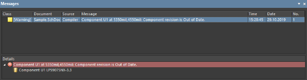
A typical PCB error message box contains several key elements:
- Error Severity Indicator: Usually represented by an icon (red for errors, yellow for warnings, blue for information)
- Error Code/ID: A unique identifier for the error type (e.g., DRC-1024)
- Error Description: A human-readable explanation of the issue
- Location Information: Coordinates or component references where applicable
- Rule Reference: Which design rule was violated
- Suggested Actions: Potential solutions or next steps
- Navigation Options: Buttons like “Ignore,” “Ignore All,” “Fix,” or “Help”
Common Causes of PCB Error Messages
Understanding the root causes of error messages helps prevent them in future designs:
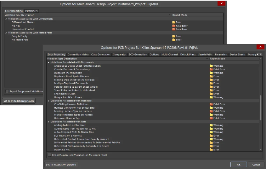
1. Incorrect Design Rule Setup
Many errors stem from improperly configured design rules. For example:
- Setting clearance rules too tight for manufacturing capabilities
- Specifying incorrect layer stackup parameters
- Defining inappropriate via size rules
2. Schematic-to-PCB Synchronization Issues
Common synchronization problems include:
- Component parameter mismatches between schematic and PCB
- Netlist generation errors
- Annotation inconsistencies
3. Library Management Problems
Library-related issues often cause errors:
- Using outdated or non-standard component libraries
- Missing library references when sharing files
- Corrupted library files
4. Design Complexity Challenges
As designs become more complex, new error sources emerge:
- High-speed design constraints violations
- Impedance control mismatches
- Signal integrity rule violations
Strategies for Resolving PCB Error Messages
1. Systematic Error Resolution Approach
Develop a methodical process for handling errors:
- Categorize: Determine if the error is critical or can be deferred
- Prioritize: Address manufacturing-critical errors first
- Document: Keep records of recurring errors and their solutions
- Verify: Confirm fixes don’t introduce new issues
2. Understanding False Positives
Not all errors require fixing—learn to identify false positives:
- Intentional rule violations for specific design requirements
- Temporary violations during editing that will resolve naturally
- Non-critical warnings that don’t affect functionality
3. Utilizing Error Navigation Tools
Modern PCB software offers powerful error navigation:
- Cross-probing between error messages and design locations
- Batch error resolution tools
- Error filtering and grouping capabilities
4. Implementing Preventive Measures
Reduce errors through proactive measures:
- Create and use standardized design templates
- Develop comprehensive design rule sets
- Establish component library management protocols
- Implement design review checkpoints
Advanced Error Handling Techniques
1. Custom Design Rule Configuration
Advanced designers can:
- Create application-specific design rules
- Set up conditional design rules
- Define rule hierarchies and priorities
2. Scripting and Automation
For repetitive error resolution:
- Develop scripts to automatically fix common error types
- Create macro sequences for bulk operations
- Implement custom error checking routines
3. Integration with Version Control
Manage errors across design iterations:
- Track error introduction and resolution across versions
- Implement design freeze points for error review
- Use branching for experimental error resolution attempts
Best Practices for Error Message Management
1. Organizational Standards
Establish company-wide protocols for:
- Error message documentation
- Resolution workflow
- Escalation procedures for complex issues
2. Continuous Learning
Maintain and share knowledge about:
- Common error patterns in your designs
- Effective resolution techniques
- Software-specific error handling features
3. Vendor Collaboration
Work with software vendors to:
- Report unclear or unhelpful error messages
- Suggest improvements to error detection
- Understand planned error handling enhancements
Future Trends in PCB Error Handling
The evolution of PCB design software continues to improve error handling:
1. AI-Assisted Error Resolution
Emerging technologies include:
- Machine learning-based error prediction
- Intelligent auto-correction suggestions
- Context-aware error prioritization
2. Enhanced Visualization
Improved error representation through:
- 3D error visualization
- Augmented reality error highlighting
- Interactive error exploration
3. Cloud-Based Error Analysis
Future systems may offer:
- Crowd-sourced error resolution databases
- Real-time error pattern recognition across multiple designs
- Collaborative error resolution platforms
Conclusion
PCB error message boxes, while sometimes frustrating, serve as essential guardians of design quality and manufacturability. By developing a deep understanding of these messages—their causes, implications, and resolution methods—designers can significantly improve their workflow efficiency and output quality. The key lies in treating error messages not as obstacles, but as valuable feedback that helps create better PCB designs.
As PCB technology continues to advance with higher densities, faster signals, and more complex architectures, the role of error detection and handling will only grow in importance. Designers who master the art of interpreting and resolving PCB error messages will find themselves at a significant advantage in producing reliable, high-quality boards in less time and with fewer iterations.
Remember that effective error management is not just about fixing problems as they arise, but about developing design practices that prevent errors from occurring in the first place. By combining careful design methodology with thorough error checking and resolution techniques, PCB professionals can minimize design re-spins, reduce time-to-market, and ultimately create better electronic products.