The Role and Addition Methods of Teardrops in PCB Design
Abstract
In printed circuit board (PCB) design, teardrops are small, tapered connections between pads and traces or vias and traces that enhance reliability and manufacturability. This article explores the significance of teardrops in PCB design, their benefits, and various methods to add them using modern electronic design automation (EDA) tools.
1. Introduction
PCB design involves intricate routing of traces between components, vias, and pads. One common challenge is ensuring strong mechanical and electrical connections at junctions where traces meet pads or vias. Teardrops help mitigate potential manufacturing defects by reinforcing these critical points.
2. What Are Teardrops?
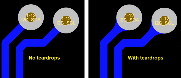
Teardrops are small, tapered fillets added at the junction of a trace and a pad or via. They resemble a drop of water, hence the name “teardrop.” Their primary purpose is to provide a smooth transition between the trace and the pad/via, reducing stress concentration and improving structural integrity.
2.1. Structure of a Teardrop
A typical teardrop consists of:
- A wider base where the trace connects to the pad/via.
- A gradual taper that narrows down to the trace width.
- A smooth curvature to avoid sharp angles.
3. Benefits of Using Teardrops in PCB Design
3.1. Improved Mechanical Strength
During PCB fabrication and assembly, mechanical stresses (such as drilling and thermal cycling) can weaken connections. Teardrops reinforce these points, reducing the risk of cracks or breaks.
3.2. Enhanced Electrical Reliability
Poor connections can lead to increased resistance or intermittent failures. Teardrops ensure a more consistent copper distribution, improving current flow and signal integrity.
3.3. Better Manufacturability
In high-precision PCBs (e.g., HDI designs), teardrops help prevent acid traps—areas where etching chemicals might accumulate and over-etch the copper, leading to weak spots.
3.4. Reduced Signal Reflection
In high-frequency designs, abrupt impedance changes at pad-trace junctions can cause signal reflections. Teardrops provide a smoother transition, minimizing discontinuities.
4. When to Use Teardrops?
Teardrops are particularly useful in:
- High-density interconnect (HDI) PCBs.
- Flexible PCBs where mechanical stress is a concern.
- High-current or high-frequency designs.
- Designs with fine-pitch components (e.g., BGA, QFN).
5. How to Add Teardrops in PCB Design?
Most modern EDA tools support teardrop generation either automatically or manually. Below are common methods in popular PCB design software.
5.1. Automatic Teardrop Generation
Altium Designer
- Go to Tools > Teardrops.
- Configure settings such as:
- Teardrop Style (Curved or Linear).
- Size Ratio (adjusts the tapering length).
- Objects to Apply (Pads, Vias, or Both).
- Click OK to apply.
KiCad
- Install the “Teardrops” plugin via Pcbnew > Tools > External Plugins > Teardrops.
- Select the desired pads/vias and run the plugin.
Cadence Allegro
- Use the “Add Teardrop” command in the Route menu.
- Specify parameters like width and length.
5.2. Manual Teardrop Addition
If automatic tools are unavailable, designers can manually draw teardrops:
- Use a curved or tapered polygon shape.
- Ensure smooth transitions without sharp angles.
- Verify design rule checks (DRC) to avoid clearance violations.
6. Best Practices for Teardrop Implementation
- Avoid Overuse: Excessive teardrops can complicate routing in dense layouts.
- Optimize Size: Too large teardrops waste space; too small may be ineffective.
- Check DRC: Ensure teardrops do not violate clearance rules.
- Review Manufacturing Guidelines: Some PCB fabricators may have specific teardrop preferences.
7. Potential Challenges and Solutions
7.1. Increased File Size
Teardrops add extra copper shapes, which can increase Gerber file sizes. Use optimized teardrop settings to balance reliability and file complexity.
7.2. Signal Integrity in RF Designs
In some RF applications, teardrops may introduce slight impedance variations. Simulate high-frequency circuits to ensure minimal impact.
7.3. Compatibility with Older EDA Tools
Some legacy PCB software may not support automatic teardrops. In such cases, manual addition or scripting (e.g., Python scripts in KiCad) can be used.
8. Conclusion
Teardrops play a crucial role in enhancing PCB reliability, manufacturability, and performance. By understanding their benefits and applying them correctly using EDA tools, designers can significantly improve board quality. Whether through automatic tools or manual methods, incorporating teardrops should be a standard practice in modern PCB design.