
Let PCB Shielding Protect Your Design
In the 7th century BC, Greek soldiers or heavy infantry carried a large concave circular shield called a hoplon. Made of bronze and wood, the hoplon or Argive shield protected the heavy waist from chin to knees and when overlapped became the basis of the Greek phalanx.
In the early 20th century, Ethiopians fought against invading Italian armies using their shields. The Ethiopians constantly banged their shields during the war, which was a terrible prelude to battle. Ancient armies deployed shields to prevent false attacks and form war strategies. PCB designs often rely on different types of shielding to protect sensitive circuits from stray RF signals.
In these circuit outposts, rebellious wires and traces do everything they can to allow electromagnetic interference (EMI) to escape to the periphery of their domain. Those skirmishes never end. Shielding should be part of the overall PCB design strategy. Shielding and Shielding Design Shielding should not be considered an add-on feature, but should be part of the initial PCB design process.
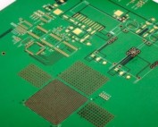
What can PCB shielding do for you?
RF front-ends, switches, and clock circuits emit EMI either through conduction paths or through radiation. Good PCB design and good shielding combine to reduce EMI. Good PCB design for EMI revolves around layout, placement of filters, and ground planes. A well-designed PCB minimizes parasitic capacitance and ground loops.
Metals, magnetic materials, and gaskets used as shields prevent EMI radiation.
Rather than providing a physical barrier sword against a spear, PCB shielding simulates a Faraday cage connected to the ground. While the ground plane forms the bottom of the cage, metal shielding can be used to form the other five sides.
Shielding causes reflection losses and absorption losses of electromagnetic energy. Reflection losses vary with the type of field and occur as air-to-shield or shield-to-air losses. Absorption losses occur when the field propagates through the shield. Absorption losses vary with the type of shielding material. The shielding effect is equal to the sum of reflection and absorption losses. Conductive barriers hide all or part of the circuit, absorb and reflect radiation from loop antennas, and create electrical isolation.
While your design may not need a Fort Knox, a chassis can help.
The concept of a shield wall became famous when Roman legions used land turtles to form. You can also use shielding to form walls to protect sensitive circuits from harmful EMI emitted by other circuits. Electromagnetic fields contain electric and magnetic fields that are oriented at 90° to each other.
If the electric field interacts with the magnetic field, propagation occurs. Shielding walls separate sections of a PCB by attenuating the electric (E-field) and magnetic (H-field) fields of radiated electromagnetic interference waves through a combination of metal and magnetic shielding.
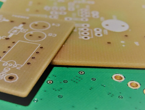
Round or square: different shielding for different PCB needs
Unlike jumpers, shielding used on PCBs does not protect from chin to knee. Hidden enemies such as aperture radiation and cavity resonance can make life difficult. Electromagnetic interference can appear everywhere. As electronic devices become smaller, shielding design emphasizes a combination of lightweight, mechanical stability, and electrical efficiency.
The shielding you choose for your PCB design depends on whether the emission is near-field or far-field, the frequency of the interference, and whether the interference occurs in electric or magnetic field interference. Each of these factors affects the choice of shielding type and thickness.
Most emissions under shielding are near-field emissions. For near-field emissions, reflection and absorption losses vary with frequency. E-field emissions caused by digital circuits have higher reflection losses at lower frequencies and higher absorption losses at higher frequencies. Switch-mode power supplies create magnetic field emissions at low frequencies with small reflection and absorption losses.
Protecting from losses inside and outside your design will keep it durable in any war.
Near-field and far-field emissions have different source characteristics and different E/H ratios. EMI is a far-field emission. Far-field sources have larger reflection losses at lower frequencies. The higher the frequency, the greater the absorption losses.
There are two key variables to consider when deciding on the type of shielding material. Conductivity measures the ability of a shielding material to conduct an electric current. Permeability measures the ability of a material to support a magnetic field formed within the material. A shield with high magnetic permeability has low magnetic resistance and can direct magnetic fields.
As with current and resistance, the lowest amount of magnetic resistance creates a path for the magnetic field. Shielding material thickness becomes an important factor for PCBs with low-frequency magnetic field applications.
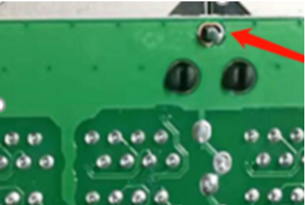
Still Needs to Breathe: Aperture Controls Shielding Effectiveness
Ancient fortresses always had a weak spot that an invading army could exploit. Good shield design also considers mechanical strength and the need for air flow. Shields include holes that reduce heat buildup by allowing air to flow through the shield openings. The number and size of the apertures in the shield design controls the effectiveness of the shield.
While many apertures will reduce efficiency, the spacing between the apertures and frequency determines the amount of reduction. In addition, the amount of leakage through the apertures depends on the largest linear dimension of the opening.