
Skip to content
Andwin Circuits
  • Home
  • ProductsExpand
    • HDI multilayer PCB
    • Rigid Flex PCB
    • Flex pcb
    • Special PCBExpand
      • High Frequency PCBExpand
        • Rogers RO4350B PCB
        • Rogers RO4003 pcb
        • Rogers RO3003 PCB
        • Rogers 5880 PCB
        • DICLAD 527 PCB
        • Taconic TLX series
        • Taconic TLX-8 RF PCB
        • Taconic TLX-9 RF PCB
      • High speed pcbExpand
        • Megtron 6 High Speed PCB
        • TU-872 SLK Sp High Speed
      • High TG PCBExpand
        • SHENGYI SH260 PCB
        • ISOLA 370HR PCB
        • ISOLA IS410 PCB
        • ISOLA IS420 PCB
      • Heavy copper PCB
      • Copper coin pcb
      • Copper inlay PCB
    • Metal Core PCBExpand
      • Copper core pcb
      • Aluminum PCB
      • 2 Layers Aluminum PCB
      • Direct thermal MCPCB
      • 2 Layers Direct Thermal
    • Ceramic PCBExpand
      • DPC ceramic PCB
      • DBC ceramic PCB
      • Thick film Ceramic PCB
      • Al2O3 Alumina PCB
      • AIN ALN ceramic PCB
      • IGBT Ceramic PCB
  • ServiceExpand
    • PCB Assembly
    • Quick turn PCB assembly
    • PCBA conformal coating
  • IndustryExpand
    • Telecommunication
    • IoT and Wireless
    • Industrial Control
    • Thermal management
    • Power and Energy
    • IC test board
    • Automative
    • Medical
  • CapabilityExpand
    • Rigid PCB
    • Rigid flex PCB
    • Metal core PCB
    • PCB Assembly
  • TechnologyExpand
    • Blogs
    • Via in pad
    • PCB E-test
    • PCB stack up
    • MCPCB panelization
    • Controlled impedance PCB
  • AboutExpand
    • About us
    • Certification
    • Factory Tour
  • Contact
Andwin Circuits
Home / PCB warpage analysis function

PCB warpage analysis function

ByGrace July 12, 2025July 10, 2025

1 Introduction

PCB is now widely used in our lives, so there is an increasing demand for product reliability. To meet this demand, we need to introduce simulation methods to improve the quality of our products, identify corresponding problems through simulation in the early stage of design, and deal with them in a targeted manner.

In our early technical articles, we elaborated in detail how to quickly model complex chips or PCB models and perform accurate simulation analysis through the trace mapping function (next article). This article will further provide new methods on the original basis to achieve more accurate analysis.

First, let us review the previous issues about PCB reliability. PCB has different working conditions such as temperature change, cutting, and vibration during the manufacturing process and actual use. How to ensure that related defects can be quickly analyzed and solved in similar environments, two key factors are modeling and material parameters.

Among them, it is very difficult to completely model such products in finite elements due to the size specifications of PCB or chips. Therefore, in the previous article, we provided the trace mapping function, which can conveniently and efficiently model the structure of PCB and accurately define the material properties of each layer of PCB, so that complex PCB products can be quickly analyzed.

2 Reinforcement

Trace mapping is a mapping function based on the metal volume fraction to reflect the material information of the stackup and via holes in the PCB. The result only reflects the deformation and stress of the corresponding model structure on this basis. When we need to locate the defect position in detail or view the detailed deformation of the stackup, this function cannot meet our requirements, so another function needs to be imported.

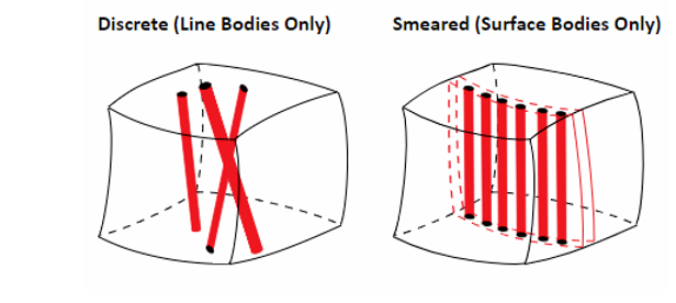
For properly modeled geometries, Mechanical provides the option of specifying reinforcement materials in the structure. Mechanical can model these enhanced geometries using special reinforcement components. These reinforcement components interact with standard structures or thermal wishes through shared nodes to provide additional reinforcement. As shown in the figure, Mechanical provides reinforcement specifications for line bodies (discrete reinforcement materials) and surface bodies (diffuse reinforcement materials). Each line body designated as a reinforcement material basically represents a reinforcement fiber arbitrarily oriented in space. Each surface body designated as a reinforcement material basically represents a reinforcement layer. The reinforcement layer can be a homogeneous reinforcement layer or a reinforcement layer with uniformly spaced fibers.
Contact us for PCB quote now |

3 Sherlock

How to add reinforcement requires the use of another Ansys software Sherlock. Sherlock is a software for life prediction analysis of PCB based on failure physical model. It is currently one of the few automated design reliability analysis software based on POF in the world. Its principle is based on the actual physical process of product failure. By constructing the corresponding mathematical model, the purpose of quantitative description and evaluation of product failure is achieved, and then the product research and development goals such as product design optimization, product reliability growth and guarantee are completed.

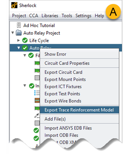
In addition to analyzing the life of the PCB, Sherlock has a special function that can generate a stackup model for each layer of the PCB, import the stackup output into the Mechanical model, model the stackup and via holes as reinforcement components in Mechanical, and when the exported model is opened in Workbench Mechanical, the following properties will be automatically applied according to the settings in Sherlock: the thickness of the trace model, the shell reinforcement element, the through-hole cross-section of the beam reinforcement element, and all corresponding material properties. The flow chart is as follows:
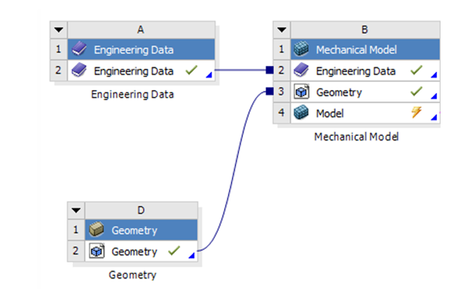
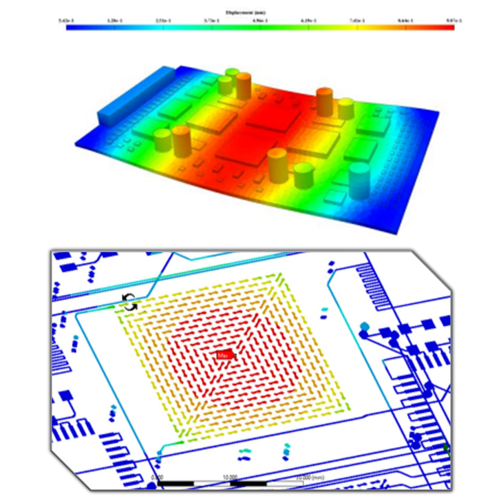
Combine the output stackup with the PCB model, and set the reinforcement unit for the imported stackup model. After combining the two, more detailed analysis results can be obtained. On this basis, we can better view the stress and deformation of the relevant stackup, as shown in the figure:
4 Conclusion

Combining Sherlock’s stackup function with trace mapping can better accurately model the PCB model and obtain more detailed results.

Contact us for PCB quote now |

Post Tags: #aluminum clad pcb#aluminum core pcb#aluminum pcb#assemble pcb#pcb warpage

Post navigation

Previous Previous
The Open-Source PCB Revolution: Exploring the Potential of Solder Mask-Free Designs
NextContinue
How to Write Text on a PCB: Techniques and Best Practices

Search

Search

Products

  • HDI Multilayer PCB
  • Rigid Flex PCB
  • Flex pcb
  • High Frequency PCB
  • High speed pcb
  • Heavy copper PCB
  • Metal Core PCB
  • Ceramic PCB

Address

Andwin Circuits Co.,Limited
Email: sales@andwinpcb.com
Tel: +86 755 2832 9394
Fax:+86 755 2992  6717
ADD:1-2F-1217,HouDeQun Industrial park,
NanTing RD NO.56,ShaJing,BaoAn,Shenzhen 518104,GuangDong,China

Products

  • HDI Multilayer PCB
  • Rigid Flex PCB
  • Flex pcb
  • High Frequency PCB
  • High speed pcb
  • Heavy copper PCB
  • Metal Core PCB
  • Ceramic PCB

Technology

  • Blogs
  • Via in pad
  • PCB E-test
  • PCB stack up
  • Metal core PCB panelization
  • Controlled impedance PCB

CERTIFICATION

Certification >>


Copyright© 2003 - 2026 Andwin | All Rights Reserved | Powered by Andwin

Scroll to top
  • Home
  • Products
    • HDI multilayer PCB
    • Rigid Flex PCB
    • Flex pcb
    • Special PCB
      • High Frequency PCB
        • Rogers RO4350B PCB
        • Rogers RO4003 pcb
        • Rogers RO3003 PCB
        • Rogers 5880 PCB
        • DICLAD 527 PCB
        • Taconic TLX series
        • Taconic TLX-8 RF PCB
        • Taconic TLX-9 RF PCB
      • High speed pcb
        • Megtron 6 High Speed PCB
        • TU-872 SLK Sp High Speed
      • High TG PCB
        • SHENGYI SH260 PCB
        • ISOLA 370HR PCB
        • ISOLA IS410 PCB
        • ISOLA IS420 PCB
      • Heavy copper PCB
      • Copper coin pcb
      • Copper inlay PCB
    • Metal Core PCB
      • Copper core pcb
      • Aluminum PCB
      • 2 Layers Aluminum PCB
      • Direct thermal MCPCB
      • 2 Layers Direct Thermal
    • Ceramic PCB
      • DPC ceramic PCB
      • DBC ceramic PCB
      • Thick film Ceramic PCB
      • Al2O3 Alumina PCB
      • AIN ALN ceramic PCB
      • IGBT Ceramic PCB
  • Service
    • PCB Assembly
    • Quick turn PCB assembly
    • PCBA conformal coating
  • Industry
    • Telecommunication
    • IoT and Wireless
    • Industrial Control
    • Thermal management
    • Power and Energy
    • IC test board
    • Automative
    • Medical
  • Capability
    • Rigid PCB
    • Rigid flex PCB
    • Metal core PCB
    • PCB Assembly
  • Technology
    • Blogs
    • Via in pad
    • PCB E-test
    • PCB stack up
    • MCPCB panelization
    • Controlled impedance PCB
  • About
    • About us
    • Certification
    • Factory Tour
  • Contact
Search