50-Layer PCB Manufacturing: Overcoming the Extreme Challenges of Ultra-High Layer Count Integration
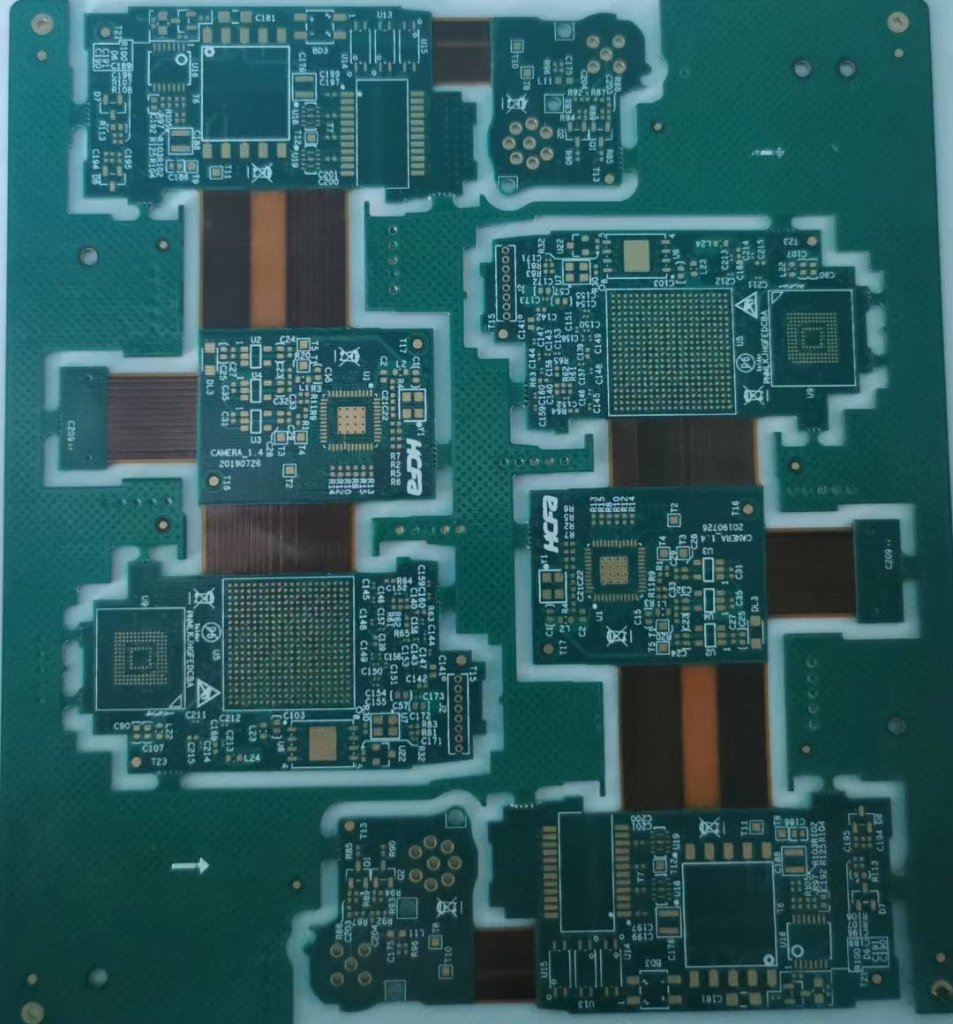
In the world of high-performance computing, aerospace telemetry, and 6G infrastructure, the demand for density has pushed PCB design to its physical limits. While a standard 12-layer board is routine for many, a 50-layer PCB represents the “Everest” of electronic manufacturing. For senior hardware engineers and procurement managers in North America and Europe, the stakes are incredibly high: a single registration error or a plating void in a $15,000 prototype can set a project back by months.
This guide dives deep into the hardcore engineering challenges of 50-layer PCB fabrication, providing data-driven insights into how elite manufacturers solve the problems of layer alignment, extreme aspect ratios, and thermal reliability.
Table of Contents
1. Understanding 50-Layer PCBs: The Basics of Extreme Integration
2. Core Concepts Simplified: The “Tall Building” Analogy
3. The Engineering Breakthroughs: How 50 Layers Become Reality
4. Expert Tips & Common Pitfalls to Avoid
5. Conclusion & Final Thoughts
1. Understanding 50-Layer PCBs: The Basics of Extreme Integration
A 50-layer PCB is not just “thicker” than a standard board; it is a complex thermodynamic system. At this scale, we are typically looking at a finished board thickness of 5.0mm to 7.0mm.
Why go this far? In supercomputing and high-end switching fabrics, the sheer volume of I/O signals requires massive routing real estate. However, as layers increase, the margin for error shrinks to near zero. For the Western engineer, the primary concern isn’t just “can you make it?” but “can you make it with signal integrity and long-term reliability?”
The transition from 20 layers to 50 layers introduces non-linear challenges in:
- Coefficient of Thermal Expansion (CTE) Mismatch: The Z-axis expansion during soldering can tear copper barrels apart.
- Signal Attenuation: Long vertical transitions (vias) act as antennas or stubs if not managed.
- Manufacturing Yield: Statistical probability dictates that if each layer has a 99% yield, a 50-layer board would have a cumulative yield of only 60%. Elite shops must achieve “Six Sigma” precision at every sub-step.
2. Core Concepts Simplified: The “Tall Building” Analogy
To understand a 50-layer PCB, imagine constructing a 50-story skyscraper on a footprint the size of a postage stamp.
- Layer Registration (The Foundation): If the 1st floor and the 50th floor are off by even a few millimeters, the elevator (the drill bit) will crash through the walls instead of the shaft.
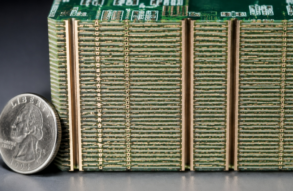
- Aspect Ratio (The Elevator Shaft): Imagine trying to paint the inside of an elevator shaft that is 20 stories deep but only 2 feet wide. This is the challenge of Extreme Aspect Ratio Drilling, where we must plate copper uniformly inside a tiny hole that spans a massive thickness.
- Sequential Lamination (The Phased Construction): You don’t build all 50 floors at once. You build 10, stabilize them, add the next 10, and so on. This is critical for advanced HDI PCB manufacturing, where microvias only connect specific sub-layers.
Technical Comparison: Standard vs. Ultra-High Layer Count
| Feature | Standard Multilayer (8-16 Layers) | Ultra-High Layer (50+ Layers) |
|---|---|---|
| Typical Thickness | 1.6 mm | 5.0 mm – 7.0 mm |
| Aspect Ratio | 8:1 to 10:1 | 20:1 to 30:1 |
| Registration Tolerance | ± 75 µm | ± 25 µm (or less) |
| Lamination Cycles | 1 Cycle | 3 to 5 Cycles (Sequential) |
| Material Requirement | Mid-Tg FR4 | Ultra-Low Loss, High-Tg (e.g., Megtron 7) |
3. The Engineering Breakthroughs: How 50 Layers Become Reality
Manufacturing a board of this complexity requires moving away from traditional “press and drill” methods toward specialized, high-precision workflows.
3.1 Advanced Layer Registration & Alignment
In a 50-layer stackup, “Inner-layer Shift” is the enemy. Traditional mechanical pinning often fails due to the cumulative material movement (shrinkage/expansion) during the high-heat lamination process.
The Solution:
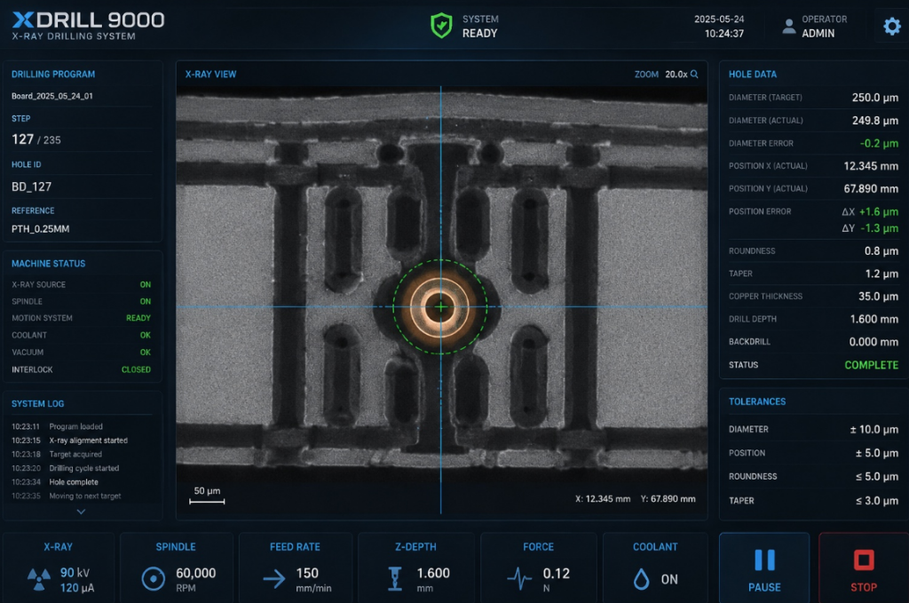
We utilize Optical Alignment Systems (OAS). Before lamination, each inner layer is scanned, and its actual dimensions are compared to the CAD data. The system then calculates the “best fit” center for the entire stack. During the build, X-ray induction drilling is used to find the internal targets, ensuring that the multilayer board reliability is maintained even at the center of the 7mm thick slab.
3.2 Extreme Aspect Ratio (AR) Drilling and Plating
When the board is 6mm thick and the drill bit is 0.25mm, you are dealing with a 24:1 Aspect Ratio.
- The Problem: Surface tension prevents the plating chemistry (electroless copper) from flowing into the center of the hole. This leads to “knee-thinning” or “voids,” where the copper is thick at the top but non-existent in the middle.
- The Solution: Pulse Plating and High-Pressure Fluid Dynamics. We use specialized equipment that vibrates the board and uses ultrasonic waves to “force” the chemistry through the holes. This ensures a minimum of 1 mil (25µm) of copper on the hole wall, even at the very center of the board.
3.3 Backdrilling: Eliminating the “Signal Echo”
In 50-layer boards, a via might go from Layer 1 to Layer 50, but the signal only needs to go from Layer 1 to Layer 10. The remaining 40 layers of copper in that hole act as a “Stub”—a dead-end wire that reflects signals back, causing jitter and EMI.
By precisely drilling out these stubs from the bottom side, we ensure the 50-layer board can handle 112G PAM4 signaling without distortion.
4. Expert Tips & Common Pitfalls to Avoid
Based on feedback from the EEVblog community and Reddit r/PrintedCircuitBoard, most 50-layer failures occur not in the layout, but in the material selection and stackup philosophy.
Pitfall 1: Ignoring the Glass Transition Temperature (Tg)
With 50 layers, the board undergoes multiple lamination cycles (Sequential Lamination). If you use a standard Tg 150°C material, the board will delaminate (split apart) by the third heat cycle.
- Pro Tip: Always specify High-Tg (180°C+) and Low CTE materials like Isola 370HR or Panasonic Megtron 6.
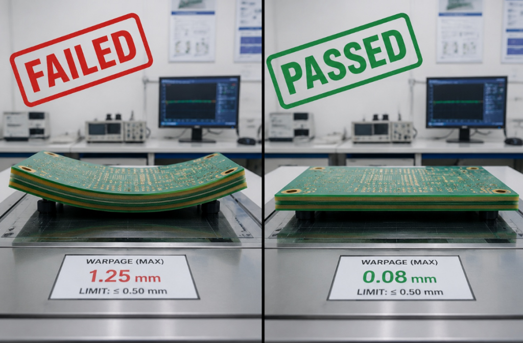
Pitfall 2: Symmetrical Stackup Neglect
A 50-layer board is prone to “Warpage” (the Pringle effect). If your copper distribution is not perfectly symmetrical around the center core, the board will twist as it cools.
- Pro Tip: Ensure that Layer 1 matches Layer 50, Layer 2 matches Layer 49, and so on, in terms of copper weight and dielectric thickness.
Pitfall 3: Thermal Relief in Ground Planes
In such a thick board, the ground planes act as a massive heat sink. If you don’t use proper thermal reliefs on your pads, you will never be able to solder components to the board—the heat from the soldering iron will be sucked away instantly.
5. Conclusion & Final Thoughts
Manufacturing a 50-layer PCB is a feat of modern engineering that requires a partnership between the designer and the fabricator. It is not a commodity product; it is a custom-engineered solution.
Key Takeaways for your next high-layer project:
- Engage Early: Talk to your manufacturer during the “Draft Stackup” phase. Don’t wait until the design is finished.
- Material is King: Don’t skimp on high-Tg, low-Dk materials. The cost of material is negligible compared to the cost of a failed 50-layer build.
- Validate Registration: Ask your vendor for X-ray registration reports and cross-section coupons for every batch.
Ready to push the limits of your next high-density project? Whether you are exploring Rigid-flex PCB design guidelines or jumping straight into 50+ layer ultra-high-density boards, precision is the only path to success.
Quick Summary Table
| Challenge | Solution | Engineering Benefit |
|---|---|---|
| Layer Offset | Optical Alignment (OAS) | Prevents internal shorts and broken nets. |
| Plating Voids | Pulse Plating / Ultrasonic Agitation | Ensures reliable Z-axis connectivity. |
| Signal Reflection | Automated Backdrilling | Enables high-speed data (112G+). |
| Warpage | Symmetrical Stackup Design | Ensures the board fits in the chassis/socket. |
Note for SEO Optimization:
The following JSON-LD structured data is provided to enhance Search Engine Results Page (SERP) visibility and is not part of the article body.