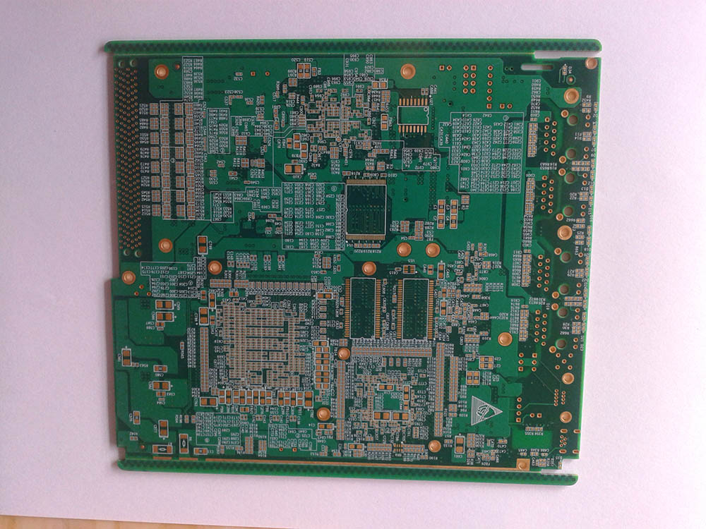
You have just routed a complex board, but there is a glaring problem: you have a high pin-count BGA, the pins are incredibly dense, and there is simply no physical space left to fan out the traces using standard through-hole vias. If you force it, you end up with a massive 12-layer board that fails EMI testing and costs a fortune. This is the exact moment you hit the wall of traditional PCB design.
The solution? High-Density Interconnect (HDI). However, transitioning to HDI introduces a steep learning curve. How do you choose between a 1+N+1 and a 2+N+2 stackup? How do you justify the higher prototyping costs to your project manager? In this guide, we will strip away the marketing fluff and use simple cross-section diagrams to explain HDI PCB technology. You will learn the exact design rules for microvias, how to decode HDI stackups, and a clear checklist to help you decide when an upgrade to HDI is absolutely necessary.
To understand the core philosophy behind HDI, think about real estate in a booming metropolis like New York or Tokyo. The land area (your PCB size) is strictly limited and cannot be expanded. However, the population (the number of component pins, especially dense BGAs) is growing exponentially.
If you build traditional single-story houses (standard through-hole vias), you will run out of space immediately. The only logical solution is to build skyscrapers reaching into the sky and subway tunnels digging underground. This allows you to pack ten times the population into the exact same square footage.
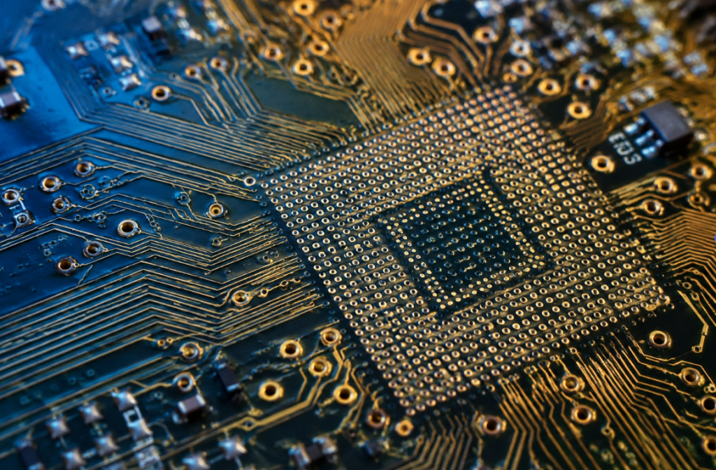
In the electronics world, HDI is that vertical architectural revolution. By utilizing microscopic laser-drilled holes and ultra-thin trace widths, HDI allows engineers to drastically increase the wiring density per unit area. If you are wondering what HDI means in PCB, it fundamentally represents a shift from mechanical drilling to laser precision, enabling the miniaturization of smartphones, wearables, and advanced aerospace electronics. It is not just about making things smaller; it is about improving signal integrity by reducing via stubs and parasitic capacitance.
Core Concepts Simplified: Vias & Microvias
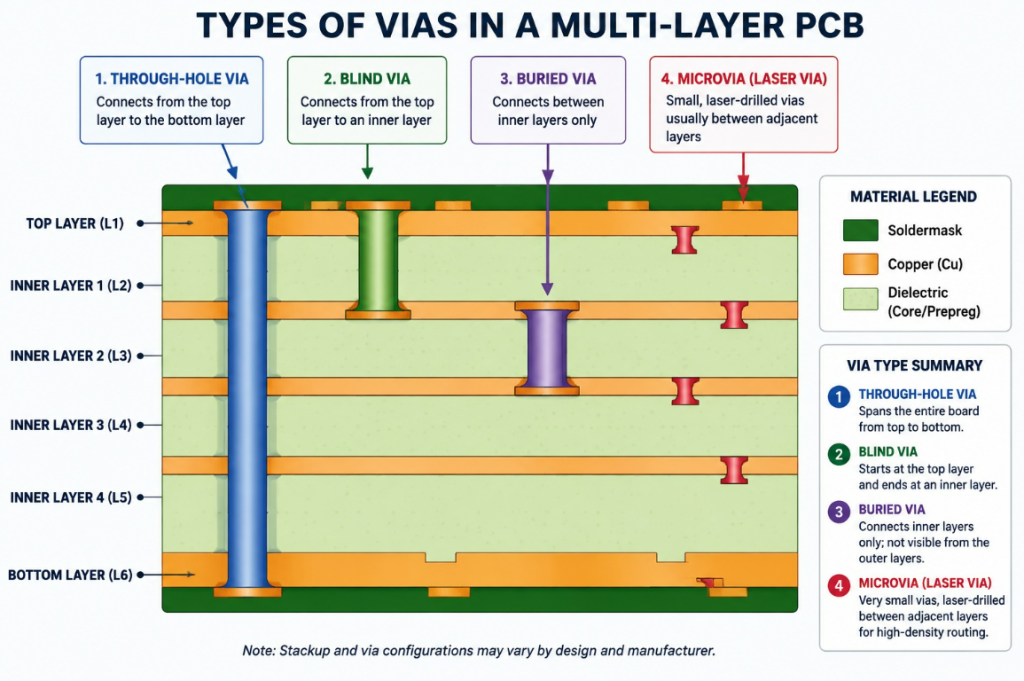
The biggest hurdle in HDI design is understanding the different types of vias. Let us use a “Multi-Layer Cake” analogy to make these technical terms crystal clear.
Through-Hole Via (The Long Straw): Imagine shoving a plastic straw straight from the top icing all the way to the bottom plate. It connects everything, but it ruins the space on every single layer of the cake, even the layers that do not need to be connected.
Blind Via (The Top Straw): A straw that is pushed into the top icing but stops halfway down. You can only see it from the outside on one side.
Buried Via (The Hidden Filling): A pocket of jam hidden entirely inside the middle layers of the cake. You cannot see it from the top or the bottom.
Microvia (The Precision Syringe): Instead of a thick straw, imagine using a microscopic needle to inject flavor exactly between two adjacent layers of the cake. In PCB terms, a microvia is created using laser ablation rather than a mechanical drill bit. It is incredibly tiny (usually <0.15mm in diameter) and typically only spans a single dielectric layer.
Via Technology Comparison Table
Feature
Standard Through-Hole
Blind / Buried Via
Laser Microvia (HDI)
Manufacturing Method
Mechanical Drill
Mechanical Drill
Laser Ablation
Typical Diameter
> 0.20 mm (8 mil)
> 0.15 mm (6 mil)
< 0.15 mm (4 mil or less)
Space Efficiency
Very Low (Occupies all layers)
Medium
Extremely High
Signal Integrity
Poor (Long via stubs cause reflections)
Moderate
Excellent (Virtually no stubs)
Cost Impact
Lowest
High (Requires extra press cycles)
Moderate to High
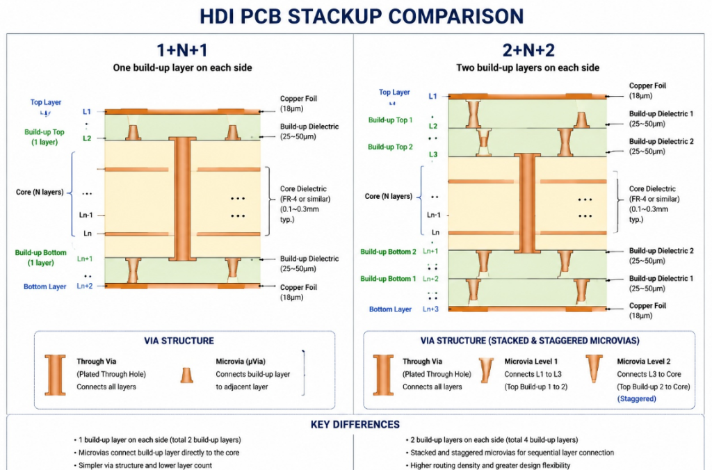
Cracking the HDI Stackup Code: 1+N+1 vs. 2+N+2
When you open a datasheet or talk to a fabricator, you will immediately be hit with terms like “1+N+1” or “2+N+2”. To non-experts, this looks like algebra. In reality, it is a very simple formula describing Sequential Lamination.
Standard PCBs are built like a sandwich: you stack all the bread, meat, and cheese at once, put it in a hot press, and bake it. HDI is built sequentially—like constructing a building floor by floor.
‘N’ represents the standard, mechanically drilled core in the center of the board.
The numbers on the outside (‘1’ or ‘2’) represent how many sequential lamination steps (adding a new outer layer and laser drilling it) are performed on each side of that core.
Scenario A: The 1+N+1 Stackup
In a 1+N+1 structure, the manufacturer takes a standard multi-layer core (N), presses one additional layer of prepreg and copper on the top, and one on the bottom. They then use a laser to drill microvias connecting layer 1 to layer 2 (and layer n to n-1).
Best for: Moderate density designs, BGAs with a pitch of 0.65mm to 0.8mm.
Pros: Cost-effective entry point into HDI. Lower manufacturing risk.
Scenario B: The 2+N+2 Stackup
If your components are even denser, one microvia layer won’t cut it. In a 2+N+2 build, after finishing the 1+N+1 step, the manufacturer adds another layer on top and bottom, and laser drills again.
Best for: High-density smartphones, wearables, and BGAs with a pitch of 0.5mm or 0.4mm.
Pros: Allows for incredibly complex routing (Fan-out) in a tiny footprint.
Cons: Every ‘+’ means another trip through the lamination press. More heat cycles mean a higher risk of material expansion issues, which significantly drives up the cost.
When Must You Upgrade to HDI? (Cost vs. Performance)
One of the most common discussions on engineering subreddits like r/PrintedCircuitBoard is how to justify the cost of HDI to management. HDI boards can cost 2x to 3x more than standard boards during the prototyping phase.
You should not use HDI just because it is modern. You should use it when physics dictates that standard manufacturing will fail. To understand the broader industry context, it helps to see why HDI PCB is used in cutting-edge electronics where form factor and weight are critical constraints.
The Decision Checklist (Spec/Data Table)
Use this table as a hard metric to decide if your project requires an HDI upgrade:
Design Constraint
Stick with Standard PCB
Upgrade to HDI Required
BGA Component Pitch
≥ 0.80 mm
≤ 0.65 mm (Mandatory for 0.4mm)
Minimum Trace / Space
4 mil / 4 mil (0.1mm)
3 mil / 3 mil or smaller
Total Layer Count
Can expand to 10-12 layers
Locked at 4-6 layers (Due to thickness limits)
High-Speed Signals
< 1 GHz
> 5 GHz (Requires stubless microvias)
Board Size Constraint
Flexible
Strictly limited (e.g., Smartwatches)
Pro Tip for Decision Making: If forcing standard vias requires you to increase your board from 6 layers to 12 layers just to complete the routing, the cost of that 12-layer standard board might actually exceed the cost of an 8-layer HDI board. Always quote both options!
Expert Tips & Common Pitfalls to Avoid
Transitioning to HDI introduces new Design for Manufacturing (DFM) rules. A common mistake made by junior layout designers is treating a microvia just like a standard via. This leads to catastrophic board failures during assembly.
Pitfall 1: Ignoring the Aspect Ratio
The Aspect Ratio is the ratio of the via’s depth to its diameter. In mechanical drilling, a 10:1 ratio is fine. In HDI, the microvia aspect ratio MUST be kept under 1:1 (ideally 0.8:1).
Why? Microvias are plated with copper using a chemical bath. If the hole is too deep and narrow, the liquid cannot flow inside, resulting in a microvia with no copper plating on the walls—creating an open circuit that is nearly impossible to debug.
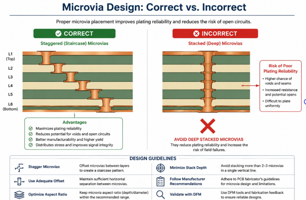
Pitfall 2: Stacking Microvias Too Deeply
In a 2+N+2 or 3+N+3 design, you have a choice on how to connect multiple microvia layers: you can Stack them directly on top of each other, or Stagger them like a staircase.
The Reddit Reality Check: Stacking microvias more than two layers deep is a massive reliability hazard. The thermal expansion (CTE) of the dielectric material will literally tear the stacked microvias apart during the reflow soldering process.
The Solution: Always use Staggered Microvias unless your fabricator explicitly guarantees the reliability of stacked structures (which usually requires expensive copper-filled microvias).
Conclusion & Final Thoughts
HDI PCB technology is not dark magic; it is simply a more precise, sequential way of building a circuit board. By replacing space-hogging through-hole vias with laser-drilled microvias, you reclaim massive amounts of routing real estate, allowing you to support ultra-dense BGA packages and high-speed signals without increasing the board footprint.
FAQ
Q1: What does HDI mean in PCB design? HDI (High-Density Interconnect) is a manufacturing technology that uses laser-drilled microvias and ultra-thin traces to pack more wiring into the same board area. It replaces bulky through-hole vias with microscopic connections, enabling smaller devices and better signal integrity.
Q2: What is the difference between 1+N+1 and 2+N+2 stackup? 1+N+1 adds one microvia layer on each side of the core—ideal for moderate density with 0.65mm pitch BGAs. 2+N+2 adds two sequential microvia layers on each side, supporting ultra-dense 0.4mm pitch BGAs in smartphones and wearables at significantly higher cost.
Q3: When must I upgrade from standard PCB to HDI? Upgrade when your BGA pitch drops below 0.65mm, your trace/space requirements hit 3 mil or smaller, your layer count is locked due to thickness limits, or your high-speed signals exceed 5 GHz. If standard vias force you from 6 layers to 12, HDI often costs less.
Q4: Why are microvias better than through-hole vias? Microvias span only one dielectric layer, eliminating long via stubs that cause signal reflections and EMI issues. They are laser-drilled to under 0.15mm diameter, freeing massive routing space compared to mechanical through-holes that block every layer.
Q5: What is the aspect ratio rule for microvias? Keep the microvia aspect ratio (depth to diameter) strictly under 1:1, ideally 0.8:1. Deeper holes prevent copper plating fluid from reaching the bottom, creating invisible open circuits that are nearly impossible to debug after assembly.
Q6: Should I stack or stagger microvias in HDI designs? Always stagger microvias like a staircase unless your fabricator explicitly guarantees stacked structures with copper filling. Stacking more than two layers deep creates a thermal expansion mismatch that tears vias apart during reflow soldering, causing latent field failures.
Quick Summary Table
Concept
Key Takeaway for Engineers
Microvias
Laser-drilled holes (<0.15mm) that save space and improve signal integrity.
1+N+1 Stackup
One layer of microvias on the outside of a standard core. Good for moderate density.
2+N+2 Stackup
Two sequential laminations. Essential for <0.5mm pitch BGAs, but costs more.
DFM Golden Rule
Keep Aspect Ratio < 1:1 and prefer staggered microvias over stacked ones.
Before you hit “Generate Gerbers” on your next high-density project, ensure your fabricator is actually capable of handling tight HDI tolerances. Partnering with a facility that specializes in HDI PCB manufacturing early in the design phase will save you from costly redesigns and guarantee that your theoretical stackup translates into a reliable physical product.
Cookie Consent
We use cookies to improve your experience on our site. By using our site, you consent to cookies.
Used to monitor number of Google Analytics server requests when using Google Tag Manager
1 minute
_ga_
ID used to identify users
2 years
_gid
ID used to identify users for 24 hours after last activity
24 hours
_gali
Used by Google Analytics to determine which links on a page are being clicked
30 seconds
_ga
ID used to identify users
2 years
__utmx
Used to determine whether a user is included in an A / B or Multivariate test.
18 months
__utmv
Contains custom information set by the web developer via the _setCustomVar method in Google Analytics. This cookie is updated every time new data is sent to the Google Analytics server.
2 years after last activity
__utmz
Contains information about the traffic source or campaign that directed user to the website. The cookie is set when the GA.js javascript is loaded and updated when data is sent to the Google Anaytics server
6 months after last activity
__utmc
Used only with old Urchin versions of Google Analytics and not with GA.js. Was used to distinguish between new sessions and visits at the end of a session.
End of session (browser)
_gac_
Contains information related to marketing campaigns of the user. These are shared with Google AdWords / Google Ads when the Google Ads and Google Analytics accounts are linked together.
90 days
__utmb
Used to distinguish new sessions and visits. This cookie is set when the GA.js javascript library is loaded and there is no existing __utmb cookie. The cookie is updated every time data is sent to the Google Analytics server.
30 minutes after last activity
__utmt
Used to monitor number of Google Analytics server requests
10 minutes
__utma
ID used to identify users and sessions
2 years after last activity
SourceBuster is used by WooCommerce for order attribution based on user source.
Name
Description
Duration
sbjs_migrations
Technical data to help with migrations between different versions of the tracking feature
session
sbjs_current_add
Timestamp, referring URL, and entry page for your visitor’s current visit to your store
session
sbjs_first_add
Timestamp, referring URL, and entry page for your visitor’s first visit to your store (only applicable if the visitor returns before the session expires)
session
sbjs_current
Traffic origin information for the visitor’s current visit to your store
session
sbjs_first
Traffic origin information for the visitor’s first visit to your store (only applicable if the visitor returns before the session expires)
session
sbjs_udata
Information about the visitor’s user agent, such as IP, the browser, and the device type
session
sbjs_session
The number of page views in this session and the current page path