Advanced 3D Stacking and Routing Techniques for Smartwatch PCB Design
In the competitive world of wearable technology, smartwatch manufacturers face a critical challenge: packing maximum functionality into minimal space. The solution lies in sophisticated 3D PCB stacking and routing techniques that enable hardware-software integration in compact form factors. This comprehensive guide explores the cutting-edge methods that power modern smartwatch design.
Understanding 3D PCB Stacking in Wearable Devices
3D PCB stacking represents a paradigm shift in wearable electronics design. Unlike traditional flat PCBs, 3D stacking involves vertically integrating multiple circuit boards or using high-density interconnect (HDI) technology to create multi-layer assemblies within extremely constrained volumes.
Modern smartwatches typically measure 40-45mm in diameter with case thickness under 12mm. Within this space, designers must accommodate processors, memory, wireless radios, sensors, batteries, and display drivers. 3D stacking achieves this by utilizing vertical space through board-on-board configurations, package-on-package (PoP) assembly, and system-in-package (SiP) integration.

The primary advantages include reduced footprint, shorter signal paths improving electrical performance, and enhanced functionality density. However, these benefits come with design challenges including thermal management, signal integrity across stacked layers, and manufacturing complexity.
Key Components of Smartwatch Hardware Architecture
A typical smartwatch PCB architecture consists of several functional blocks that must coexist harmoniously. The main processor (usually ARM-based) sits at the core, often in a PoP configuration with LPDDR memory stacked directly above.
The RF section houses multiple wireless technologies: Bluetooth Low Energy, Wi-Fi, cellular modems (LTE/5G), NFC, and GPS. Each requires careful impedance-controlled routing and often dedicated ground planes. Antenna placement becomes critical, typically using LDS (Laser Direct Structuring) antennas integrated into the watch case or frame.
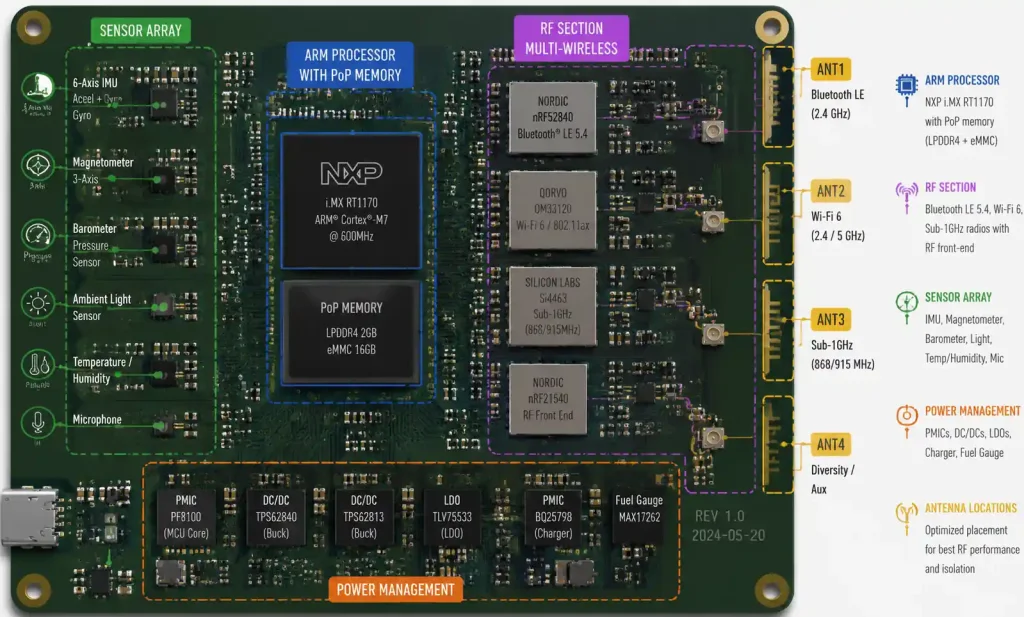
Sensor integration presents unique challenges. Modern smartwatches incorporate accelerometers, gyroscopes, heart rate monitors, blood oxygen sensors, ECG sensors, and ambient light sensors. Many connect via I2C or SPI buses, requiring careful routing to avoid crosstalk. Power management ICs (PMICs) regulate voltage rails with efficiency critical to battery life.
HDI Technology and Microvias in Compact Designs
HDI PCB technology is essential for achieving the routing density required in smartwatch designs. HDI boards use microvias (typically 0.1-0.15mm diameter) instead of traditional through-holes, allowing significantly higher interconnect density.
Smartwatch PCBs commonly employ 1+N+1 or 2+N+2 HDI stackups, where the numbers represent layers with microvias. A typical configuration might use 8-12 layers total with blind and buried vias creating interconnections between specific layer pairs.
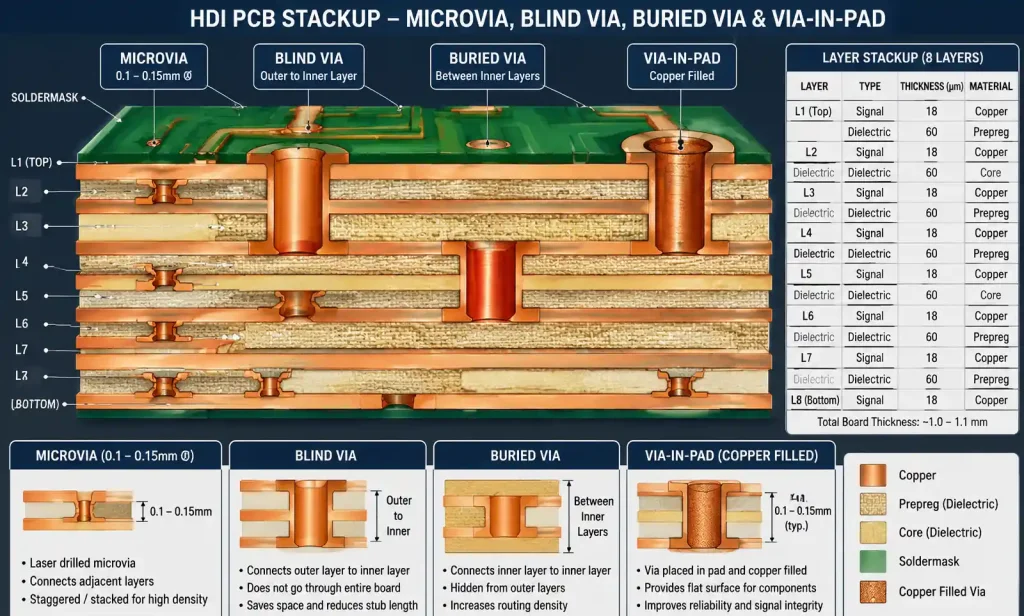
Microvia design rules differ substantially from conventional PCBs. Stacked microvias should be staggered rather than directly aligned to improve reliability. Via-in-pad technology eliminates the need for escape routing, directly connecting component pads to inner layers through filled microvias. This dramatically reduces board real estate requirements.
Laser drilling enables microvia creation with positional accuracy of ±25μm. Copper filling or conductive paste ensures reliable electrical connection while maintaining planarity for component mounting. Modern HDI processes can achieve trace widths and spacing down to 50μm/50μm, though 75μm/75μm is more common for manufacturability.
Layer Stackup Strategies for Maximum Density
Strategic layer stackup design is fundamental to successful 3D PCB routing in smartwatches. A well-designed stackup balances signal integrity, power distribution, EMI control, and routing density.
A typical 10-layer smartwatch PCB stackup might include:
- Layer 1: Component side with high-speed signals
- Layer 2: Ground plane (GND)
- Layer 3: High-speed signal routing
- Layer 4: Power plane (VDD_CORE, VDD_IO)
- Layer 5: Signal routing (I2C, SPI, GPIOs)
- Layer 6: Ground plane (GND)
- Layer 7: Signal routing
- Layer 8: Power plane (battery, PMU outputs)
- Layer 9: Signal routing
- Layer 10: Component side (back)
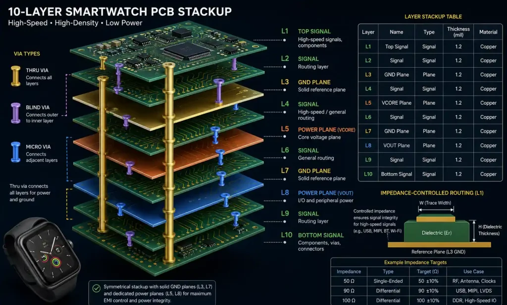
Each signal layer should be adjacent to a reference plane (ground or power) to ensure controlled impedance and minimize EMI. High-speed differential pairs (USB, MIPI) require careful impedance matching, typically 90Ω ±10% for differential pairs or 50Ω for single-ended lines.
Core thickness selection affects both impedance and manufacturing yield. Prepreg layers between copper provide the dielectric constant (typically εr = 3.8-4.5) determining impedance. Thinner cores enable more layers in the same overall thickness but increase manufacturing difficulty.
Flex-Rigid PCB Integration Techniques
Flex-rigid PCB technology represents one of the most powerful tools for smartwatch 3D design. These boards combine rigid sections for component mounting with flexible sections that fold or bend to fit irregular shapes within the watch case.
The flexible portions typically use polyimide substrates (25-50μm thick) with rolled-annealed copper for flexibility. Rigid sections use standard FR-4 material. Transition zones between rigid and flex require careful design with stiffener placement and bend radius considerations.
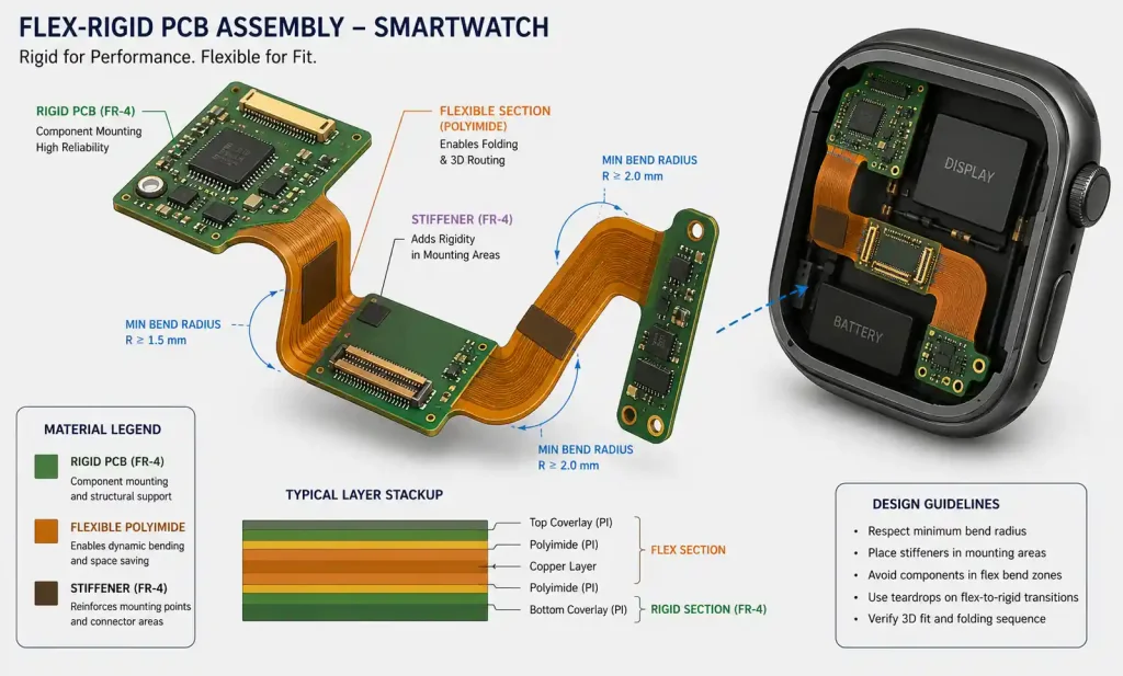
Smartwatch applications commonly employ flex sections to:
- Connect main PCB to display module
- Route signals to side buttons and crown encoders
- Interface with battery terminals
- Connect to heart rate sensor arrays on case back
Bend radius requirements dictate minimum fold dimensions, typically 6-10× the total material thickness for dynamic flexing or 3-5× for static bends. Avoiding copper traces in high-stress bend areas improves reliability, using hatched or meandered patterns where traces must cross bend zones.
Signal Integrity in Multi-Layer Stacked Designs
Signal integrity becomes increasingly critical as smartwatch PCBs pack more high-speed interfaces into smaller spaces. Modern smartwatches route USB 2.0, MIPI DSI/CSI, SPI at 50MHz+, I2C at 400kHz-3.4MHz, and various clock signals all within millimeters of each other.
Crosstalk prevention requires adequate spacing between parallel traces or using ground guard traces. The 3W rule (spacing = 3× trace width) provides basic isolation, though critical signals may need 5W or more. Differential pairs must maintain consistent spacing and length matching within 5mm typically.
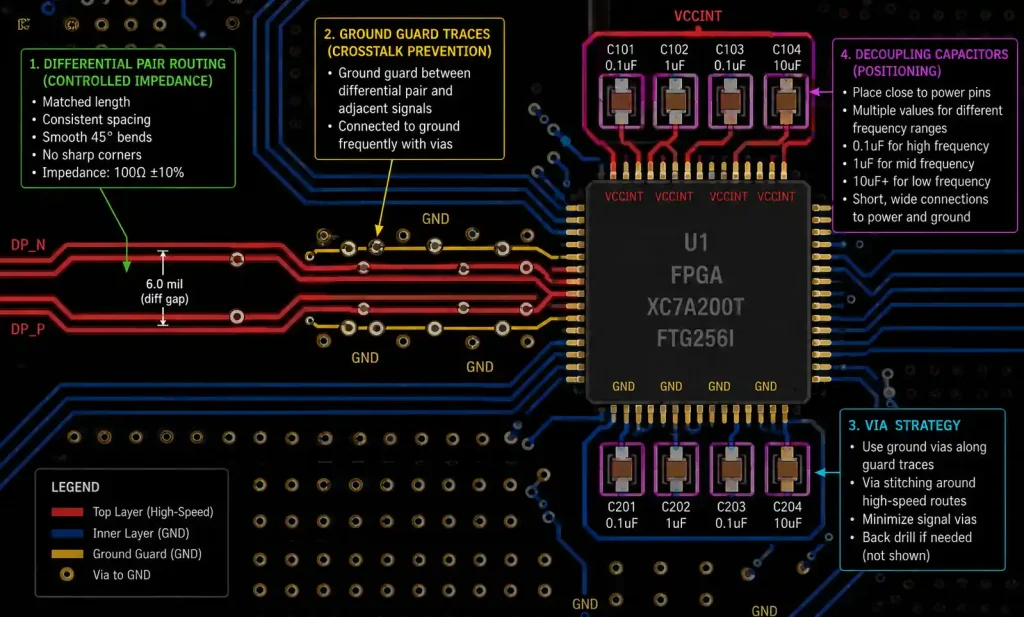
Via transitions create impedance discontinuities that reflect high-frequency signals. Minimizing via stubs, using back-drilling for high-speed traces, and adding ground vias near signal vias all improve signal integrity. GND return path continuity is essential—signal vias should always have nearby ground vias to provide low-inductance return paths.
Decoupling capacitor placement follows proximity rules: place closest to IC power pins, use multiple values (100nF, 1μF, 10μF) for different frequency ranges, and minimize trace inductance by placing vias immediately adjacent to pads.
Thermal Management in 3D Stacked Assemblies
Thermal challenges intensify in 3D stacked smartwatch designs where components generate heat in confined volumes with limited airflow. Effective thermal management is critical to performance, reliability, and user comfort.
The main processor, power management ICs, and wireless radios are primary heat sources. In 2D designs, heat spreads laterally through copper planes. In 3D stacking, heat must conduct vertically through board layers and components, creating thermal bottlenecks.
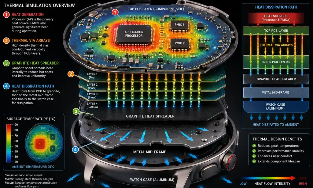
Thermal vias provide crucial heat conduction paths from hot components to external case structures. Arrays of 0.3mm thermal vias beneath processor packages conduct heat to outer layers where it dissipates to the watch case. Via fill material (epoxy or copper plating) improves thermal conductivity.
Some smartwatch designs incorporate graphite heat spreaders—thin (25-50μm) layers of highly anisotropic thermal conductivity material. These spread heat laterally across the board area before conducting to the case. Metal core PCBs or embedded copper coins provide localized thermal management for hot spots.
Component placement strategy affects thermal performance significantly. Separating heat-generating components, positioning hot components near case contact points, and avoiding stacking hot components vertically all improve thermal dissipation. Thermal simulation during design phase identifies potential issues before prototype fabrication.
Advanced Routing Techniques for Space Optimization
Routing density in smartwatch PCBs pushes the boundaries of PCB manufacturing capability. Advanced techniques maximize utilization of available routing channels while maintaining signal integrity and manufacturability.
Via-in-pad technology, mentioned earlier, represents one crucial technique. By placing vias directly in component pads (particularly BGA packages), designers eliminate escape routing that would consume valuable board area. Vias must be filled and planarized to prevent solder wicking during assembly.
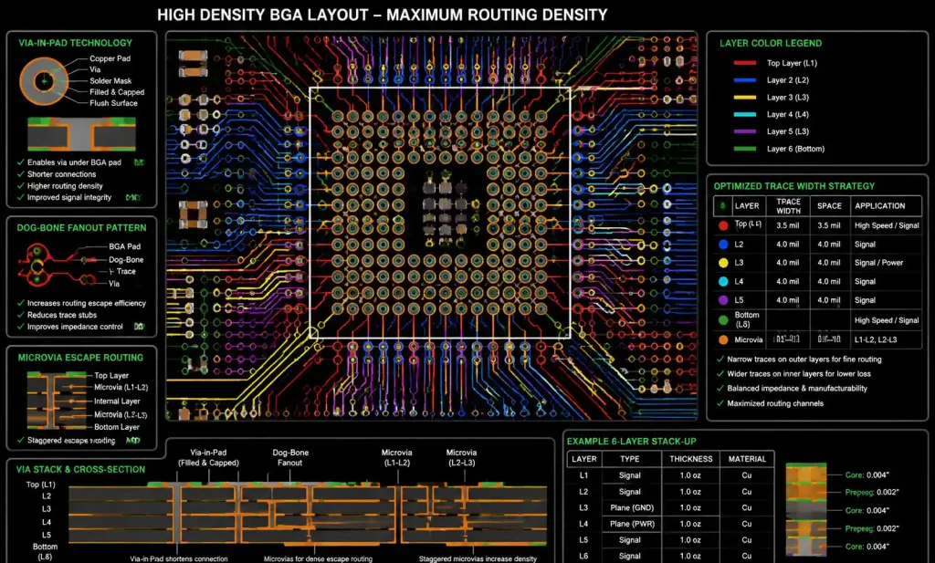
Dog-bone fanout patterns connect BGA balls to routing layers with minimal space. For 0.4mm pitch BGAs, microvias enable escape routing between pads. For even finer pitches, multiple HDI layers may be required to fan out all connections.
Cavity PCB designs create recessed areas where components sit partially within the board thickness, reducing overall assembly height. This works well for passive components like capacitors and resistors in non-critical areas.
Trace width optimization balances current carrying capacity with routing density. Power traces require wider geometries based on current requirements (typically 1A per 1mm width for 1oz copper), while signal traces can use minimum widths. Necking traces only where necessary preserves routing channels.
Manufacturing Considerations and Design for Assembly
Even the most elegant 3D PCB design fails if it cannot be reliably manufactured. Design for Manufacturing (DFM) principles become especially critical in complex smartwatch PCB designs.
HDI manufacturing capabilities vary by fabricator. Verify minimum trace/space, microvia size, aspect ratios, and registration tolerances before finalizing designs. Standard HDI processes achieve 75/75μm trace/space, while advanced processes reach 50/50μm at higher cost.
Layer registration tolerances affect microvia reliability. Blind vias connecting layers 1-3 must account for potential ±75μm misregistration between layers. Design rules should ensure adequate annular ring even with worst-case misalignment.
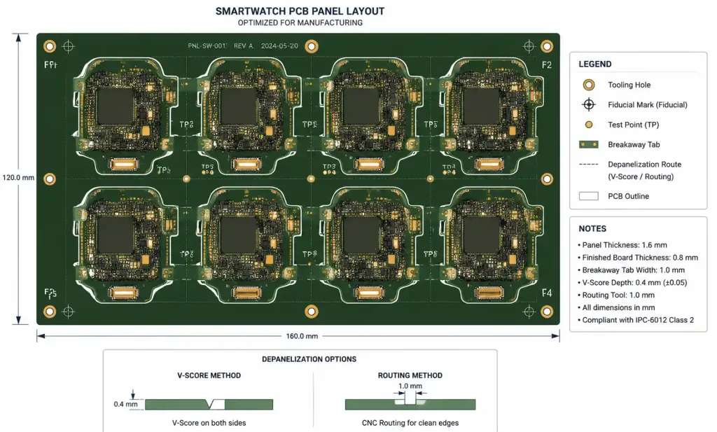
Panel utilization impacts cost significantly. Design board outlines to maximize panels, typically 18×24″ or 21×24″. Tooling holes, fiducials, and test points must fit within panel borders. Depanelization method (routing, V-scoring, or laser cutting) affects edge design.
Assembly process considerations include:
- Component placement sequence (tall components last)
- Reflow profile compatibility for all components
- Test point accessibility for in-circuit testing
- Conformal coating or underfill requirements
- Rework accessibility for failure analysis
Testing and Validation of 3D Stacked PCBs
Comprehensive testing validates that 3D stacked smartwatch PCBs meet electrical, mechanical, and reliability requirements. Testing strategies must address the unique challenges of compact, multi-layer assemblies.
Electrical testing begins with bare board testing—flying probe or bed-of-nails fixtures check continuity, isolation, and impedance. HDI boards with buried structures may require specialized test strategies since not all nets have accessible test points.
After assembly, functional testing verifies all subsystems: processor boot, memory operation, wireless connectivity, sensor functionality, and power management. Boundary scan (JTAG) testing accesses internal chip states without physical probing.
Environmental testing exposes weaknesses in thermal management, mechanical design, and moisture resistance. Thermal cycling (-40°C to +85°C), humidity exposure (85%RH/85°C), mechanical shock, and vibration testing simulate years of use in accelerated time frames.
Signal integrity validation uses high-speed oscilloscopes and vector network analyzers to measure eye diagrams, jitter, and impedance. Time-domain reflectometry (TDR) identifies impedance discontinuities that could cause signal degradation.
Reliability testing for wearables must address flex-rigid bend cycles, drop testing, and long-term wear simulation. Accelerated life testing under elevated temperature and voltage stress identifies potential failure modes before production.
Conclusion
3D PCB stacking and advanced routing techniques have revolutionized smartwatch design, enabling unprecedented functionality in remarkably compact form factors. Success requires mastering HDI technology, strategic layer stackup design, flex-rigid integration, signal integrity principles, and thermal management strategies.
As wearable devices continue evolving with more sensors, faster processors, and enhanced connectivity, these techniques will only grow more critical. Designers who understand and apply these principles will lead the next generation of smartwatch innovation, creating devices that seamlessly blend advanced technology with comfortable, elegant wearability.
The future of smartwatch PCB design lies in even greater integration—true 3D packaging with die stacking, embedded actives, and advanced packaging technologies that blur the lines between PCB and semiconductor packaging. For now, the techniques outlined in this guide represent the state of the art in wearable electronics design.