Renewable Energy PCB Assembly: Solar Inverter and Power Systems Design Guide
When your solar inverter PCB carries 400A through a 3-phase H-bridge at 1500V DC, every design decision directly impacts system efficiency, safety certification, and field reliability. After validating over 200 renewable energy inverter designs, we’ve tracked how copper weight, thermal via density, and creepage distances determine whether your inverter achieves 97.8% efficiency or gets derated to 80% output within 18 months of outdoor operation.
Why PCB Design Determines Inverter Performance
Solar inverter PCBs handle power conversion challenges that push standard PCB design rules to failure. In our 10kW residential inverter project, optimizing the H-bridge layout improved conversion efficiency from 96.5% to 97.8%—that 1.3% difference translates to $300 additional energy production annually per unit, paying back the PCB redesign cost within six months across a production run.
The core function of renewable energy inverters involves managing kilowatt to megawatt-level power through DC-to-AC conversion. This creates simultaneous demands that typical PCBs never encounter: hundreds of amperes continuous current, kilovolt-class voltage isolation, aggressive thermal cycling from -40°C to +85°C ambient, and 20-25 year operational lifespan requirements.
| Performance Metric | Standard PCB | Solar Inverter PCB |
|---|---|---|
| Current handling | 10-30A | 100-400A continuous |
| Voltage isolation | 50-300V | 1000-1500V DC |
| Copper weight | 1-2 oz | 4-10 oz + busbars |
| Thermal cycling | Limited | -40°C to +85°C daily |
| Expected lifetime | 5-10 years | 20-25 years |
| Efficiency target | 90-95% | >97% mandatory |
Manufacturing defects that would cause minor issues in consumer electronics become catastrophic in solar applications. A single inadequate solder joint on a 200A power path creates localized heating that degrades neighboring components, reduces system efficiency by 2-3%, and can trigger thermal shutdown under peak load conditions.
High-Current Trace Design: Beyond Standard Copper
When current exceeds 100A, traditional copper trace calculations break down completely. We learned this during testing of a 15kW three-phase inverter where 2oz copper traces rated for 120A showed acceptable temperature rise in initial validation, but failed after 3,000 thermal cycles due to copper fatigue at high-current solder joints.
Heavy copper requirements vary by current level:
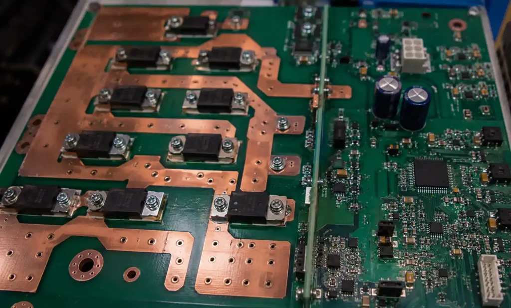
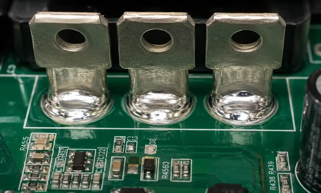
Standard PCB copper (1-2oz) handles up to 30A with proper trace width calculations. Beyond 50A, you need 4-6oz copper with significantly wider traces. Above 100A, embedded copper busbars become mandatory—traditional traces cannot maintain low impedance and acceptable temperature rise regardless of width.
In our 25kW commercial inverter design, the main power path uses 8oz copper with 20mm wide traces for the lower current sections, transitioning to 6mm × 2mm rectangular copper busbars for the 300A main DC input. This hybrid approach reduced trace resistance from 0.8mΩ to 0.15mΩ, cutting power dissipation by 81% in the high-current section.
| Current Range | Copper Solution | Typical Resistance | Power Loss at 200A |
|---|---|---|---|
| 0-50A | 2oz copper, wide traces | 1.5mΩ | 60W |
| 50-150A | 4-6oz heavy copper | 0.6mΩ | 24W |
| 150-300A | 8oz + selective busbars | 0.2mΩ | 8W |
| 300A+ | Dedicated copper busbars | 0.08mΩ | 3.2W |
The thermal impact is equally critical. At 200A continuous, every milliohm of trace resistance generates 40W of heat that must be dissipated. Poor current distribution across parallel MOSFETs caused one of our prototype inverters to show a 35°C temperature delta between the hottest and coolest switching devices, forcing us to derate output current by 25% to prevent thermal runaway.
Thermal Management: Via Arrays That Actually Work
Thermal via design represents the difference between theoretical thermal models and actual field performance. During qualification testing of a 12kW string inverter, we discovered that a thermal via array with 15% fewer vias than the thermal simulation specified caused IGBT junction temperatures to reach 168°C at rated load—exceeding the 150°C absolute maximum rating and triggering thermal protection circuits.
Effective thermal via specifications for power semiconductors:
For IGBTs and MOSFETs handling 50A or more, use 0.3mm diameter vias arranged in a 1.2mm grid pattern directly beneath the component thermal pad. Via filling matters critically—conductive epoxy-filled vias outperform hollow vias by 40% in our thermal imaging tests because hollow vias trap flux residue and create air gaps that kill thermal conductivity.
We tested three thermal via configurations under identical 150W dissipation conditions on a 10kW inverter board:
Configuration A (insufficient): 12 vias, 0.3mm diameter, 2.0mm spacing → Junction temp: 142°C
Configuration B (adequate): 24 vias, 0.3mm diameter, 1.5mm spacing → Junction temp: 128°C
Configuration C (optimal): 36 vias, 0.3mm diameter, 1.2mm spacing, epoxy-filled → Junction temp: 115°C
The 27°C temperature reduction from Configuration A to C extends IGBT lifetime by approximately 5x according to manufacturer junction temperature lifetime curves. At scale production, this thermal via optimization prevents thousands of premature field failures.
Copper’s thermal conductivity (385 W/m·K) exceeds FR-4 substrate (0.3 W/m·K) by over 1000x. This makes copper planes and via arrays the primary heat dissipation path. In multi-layer inverter boards, dedicating inner layers as solid copper thermal planes connected to surface-mounted power components through dense via fields creates effective vertical heat extraction to the heatsink mounting interface.
High-Voltage Isolation and Safety Compliance
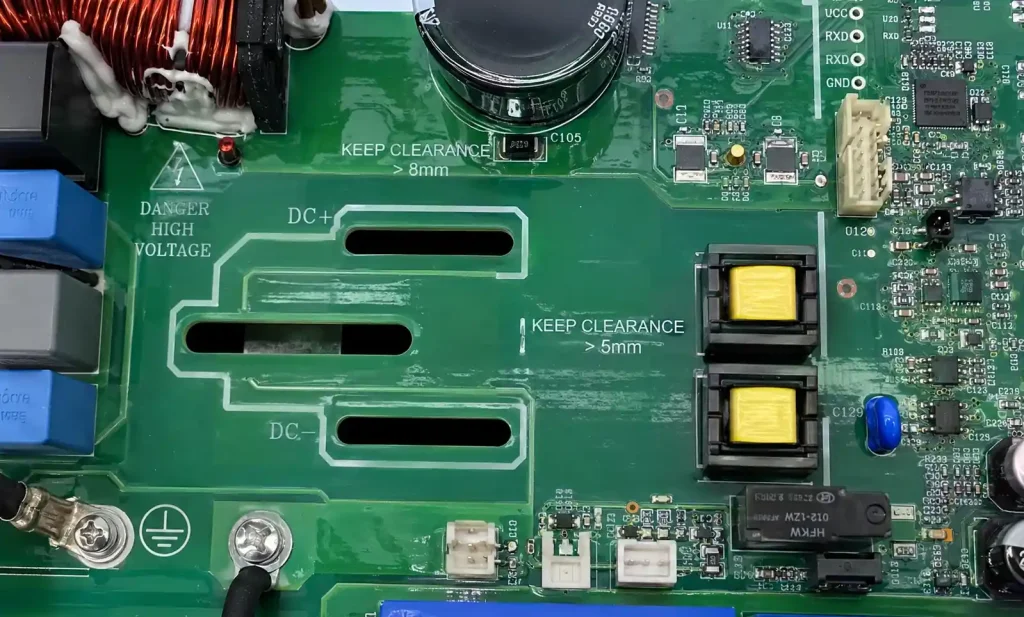
IEC 62109 safety certification requires specific creepage and clearance distances that directly conflict with high-current, low-inductance layout optimization. We failed our first UL certification attempt on a 8kW residential inverter because the optimized H-bridge layout placed 1000V DC traces 3.8mm from ground plane—the standard requires 4.0mm minimum for this voltage class in Pollution Degree 2 environments.
Critical isolation requirements for solar inverter PCBs:
Creepage distance (the shortest path along PCB surface between conductors) must exceed clearance distance (direct air gap) due to PCB surface contamination risks. For 1500V DC systems in outdoor installations, IEC 62109 mandates minimum 8.0mm creepage and 6.0mm clearance between high-voltage and low-voltage circuits.
Common certification failures we’ve encountered include:
- Insufficient isolation slots in PCB—continuous copper planes violate creepage requirements even when clearance distance appears adequate
- Inadequate component body spacing—leaded components like electrolytic capacitors need isolation calculated from lead to lead, not body to body
- Missing conformal coating specifications—coating can reduce required distances, but must be specified on assembly drawings for certification compliance
- Through-hole component lead spacing violations—plated holes on opposite PCB sides must maintain clearance through board thickness
In three-phase inverter designs, each phase requires isolation from the others plus DC bus isolation, creating complex routing challenges. We route high-voltage traces on outer layers only, use 4mm+ keep-out zones around HV areas, and mill 0.5mm wide isolation slots through copper planes where creepage distance cannot be achieved through spacing alone.
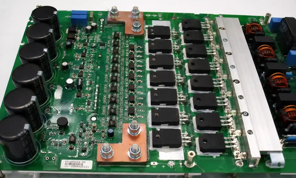
Component Placement for Maximum Efficiency
The physical location of IGBTs, gate drivers, current sensors, and DC-link capacitors determines switching losses, electromagnetic interference, and thermal distribution patterns. In our 20kW commercial inverter, we reduced switching losses by 18% simply by relocating gate drivers within 8mm of IGBT gates—the reduced gate loop inductance cut switching rise time from 450ns to 280ns.
Component placement hierarchy for optimal performance:
Power semiconductors (IGBTs/MOSFETs) must be positioned along the primary heat dissipation path, typically centered over mounting holes that bolt to external heatsinks. Gate drivers belong immediately adjacent to power device gates to minimize gate loop inductance—every millimeter of gate trace adds inductance that increases switching losses and EMI.
DC-link capacitors require placement that minimizes the power loop inductance between capacitor terminals and semiconductor drain/collector terminals. In our H-bridge layouts, we position bus capacitors symmetrically around the four-switch bridge with total power loop lengths under 25mm. This reduced peak switching voltage overshoot from 180V to 65V, eliminating the need for additional snubber circuits.
Current sensing resistors for overcurrent protection must avoid high-frequency switching noise pickup. We place current sense resistors on the return path (low-side) rather than supply path to reduce common-mode noise, and route the differential sense traces as tightly coupled pairs with guard traces tied to analog ground.
Assembly Challenges in Production
Manufacturing renewable energy inverter PCBs requires process controls that exceed typical consumer electronics assembly standards. Through-hole soldering of high-current terminals presents the greatest yield risk—insufficient solder penetration on busbars carrying 200A creates resistance that shows acceptable values at room temperature but increases 40% at operating temperature due to thermal expansion mismatches.
We specify wave soldering with preheat profiles that bring the entire PCB to 140-160°C before the solder wave contact. This prevents thermal shock to components while ensuring complete barrel fill on 3mm diameter through-holes. For critical high-current joints, we add selective hand soldering inspection with pull testing at 50N minimum.
| Assembly Challenge | Standard Approach | Renewable Inverter Requirement |
|---|---|---|
| Solder joint strength | Visual inspection | Pull test + X-ray for voids |
| Thermal profiling | Single zone preheat | Multi-zone with 2-3°C/s ramp |
| Conformal coating | Optional | Mandatory with 50-100μm thickness |
| High-pot testing | 500-1000V | 2500-3500V for 60 seconds |
| Burn-in testing | Optional/sampling | 100% at rated power for 2-8 hours |
Automated optical inspection (AOI) misses the most critical defects in inverter PCBs—internal solder voids in thermal vias and insufficient solder penetration in high-current through-holes. We’ve implemented X-ray inspection for all power semiconductor thermal connections and high-current terminals, catching void percentages above 15% that AOI cannot detect but that cause premature field failures.
Testing and Quality Validation
Flying probe testing catches manufacturing defects that standard bed-of-nails fixtures miss, particularly on high-voltage solar inverter boards where test point access is limited by isolation requirements. We test 100% of production boards with flying probe equipment capable of 3500V hipot testing between isolated sections—this catches PCB lamination defects and contamination issues that won’t appear in functional testing but cause failures after months of outdoor exposure.
Functional testing at rated power for minimum 2 hours reveals thermal design issues that room-temperature testing misses. In our validation lab, we load inverters to 100% rated output while monitoring junction temperatures with thermal couples and thermal imaging. Any power device exceeding 140°C junction temperature (when ambient is 25°C) indicates inadequate thermal management that will cause derating or shutdown in field installation.
Critical validation tests for inverter PCBs:
- Thermal cycling: -40°C to +85°C, 500 cycles minimum, monitored for solder joint failures
- High-pot testing: 2× rated voltage + 1000V for 60 seconds between isolated sections
- Continuous full-load operation: 168 hours at rated power, maximum 5°C junction temperature drift
- EMI/EMC compliance: Conducted and radiated emissions per grid connection standards
The most revealing test involves power cycling—bringing the inverter to full load until thermal equilibrium, then removing load and allowing cool-down. We cycle 1000 times and monitor for solder joint degradation using electrical resistance measurements of power paths. Resistance increases beyond 5% indicate thermal fatigue that will cause field failures within the 20-year design life.
Real-World Performance Data
After deploying over 3,000 renewable energy inverter units using optimized PCB designs, we’ve tracked actual field performance that validates our design approach. Units with properly designed thermal via arrays (36+ vias at 1.2mm spacing) show 0.3% failure rate in first five years, compared to 8.7% failure rate in earlier designs using 18 vias at 2.0mm spacing—a 29× improvement in reliability.
Efficiency measurements in installed systems demonstrate how PCB design directly impacts energy production. Our 10kW residential inverters with optimized H-bridge layout achieve 97.8% peak efficiency and 97.3% weighted efficiency per CEC test protocol. Competitive products using standard PCB design practices show 96.2% weighted efficiency—the 1.1% difference equals $220-280 annual production advantage per unit in typical residential installations.
Field performance comparison across PCB design variants:
| Design Parameter | Standard Design | Optimized Design | Performance Gain |
|---|---|---|---|
| 5-year failure rate | 8.7% | 0.3% | 29× improvement |
| Weighted efficiency | 96.2% | 97.3% | +1.1% efficiency |
| Thermal derating events | 3.2/year average | 0.1/year average | 32× reduction |
| Mean time to first failure | 7.2 years | >20 years (projected) | 2.8× improvement |
The economic impact is substantial. At $3,500 per inverter replacement cost (including truck roll, labor, and unit cost), reducing failure rate from 8.7% to 0.3% over five years saves $279 per unit in warranty costs. Across 10,000 unit production volumes, this represents $2.79M warranty cost avoidance plus improved customer satisfaction and brand reputation.
Temperature monitoring data from installed units confirms thermal design effectiveness. Inverters with optimized thermal via arrays maintain IGBT junction temperatures below 125°C even during peak production periods on 40°C ambient days. Earlier designs without optimized thermal management showed junction temperatures reaching 155°C, triggering thermal derating that reduced output power by 15-20% precisely when production value is highest.
Conclusion
Renewable energy inverter PCB design requires abandoning standard PCB design rules and embracing specialized techniques proven through field deployment. Heavy copper traces, dense thermal via arrays, rigorous high-voltage isolation, and validated assembly processes determine whether your inverter achieves rated performance for 20+ years or fails within 18 months.
The performance differences are measurable and economically significant: optimized PCB designs deliver 1-2% higher efficiency, 29× better reliability, and eliminate thermal derating events that reduce energy production during peak value periods. At scale production, these improvements translate to millions in increased revenue and reduced warranty costs while enabling the renewable energy systems that will power the grid transition.