10 Key Factors to Consider When Selecting Flexible PCB: A Practical Guide for 2026
Flexible PCBs have revolutionized electronics design, but choosing the right flex circuit for your application requires careful consideration of multiple technical and commercial factors. Based on our experience manufacturing over 500,000 flexible circuits annually, this guide walks through the critical decision points that separate successful projects from costly redesigns.
Base Material Selection: Polyimide vs Polyester
The substrate material fundamentally determines your flexible PCB’s performance envelope. In our automotive projects, we default to polyimide for under-hood applications because it maintains mechanical stability at 180°C continuous operation, while polyester degrades above 105°C.
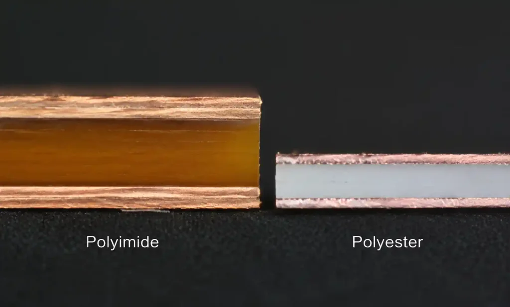
Polyimide (PI) delivers superior thermal performance with a glass transition temperature (Tg) of 360°C and continuous operating range from -200°C to +250°C. This thermal margin proves critical in applications experiencing repeated thermal cycling—we’ve documented polyester circuits failing after just 200 cycles between -40°C and 85°C, while polyimide equivalents exceed 2,000 cycles.
Polyester (PET) makes economic sense for consumer electronics with controlled thermal environments. At roughly 40-50% the cost of polyimide, PET enables cost-sensitive products like disposable medical sensors or consumer wearables operating below 80°C. However, its dimensional stability suffers—expect 0.3-0.5% shrinkage during processing compared to polyimide’s 0.05-0.1%.
| Property | Polyimide (PI) | Polyester (PET) |
|---|---|---|
| Operating Temperature | -200°C to +250°C | -70°C to +105°C |
| Glass Transition (Tg) | 360°C | 78-80°C |
| Dimensional Stability | ±0.05-0.1% | ±0.3-0.5% |
| Relative Cost | 1.0× (baseline) | 0.4-0.5× |
| Chemical Resistance | Excellent | Moderate |
| Typical Applications | Automotive, aerospace, industrial | Consumer electronics, disposables |
Key consideration: Liquid Crystal Polymer (LCP) has emerged as a third option for high-frequency applications above 20 GHz. We’re increasingly specifying LCP for 5G antenna modules due to its exceptionally low dielectric loss (dissipation factor <0.002 at 10 GHz), though it costs 1.5-2× more than polyimide.
Bend Radius and Flexing Cycles
Flexible PCB failure analysis reveals that 60-70% of field failures stem from inadequate bend radius specifications. The fundamental rule: minimum static bend radius should be at least 10× the total circuit thickness for single-flex applications.
For a typical 2-layer flex circuit with 0.1mm (4 mil) substrate and 0.035mm (1 oz) copper, the minimum static bend radius calculates to approximately 2.7mm. However, for dynamic flexing applications—where the circuit flexes repeatedly—we specify minimum bend radius of 20-25× total thickness, pushing that same circuit to 5.4-6.8mm minimum radius.
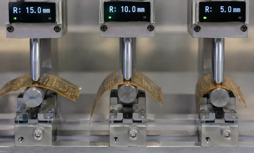
The relationship between bend radius and cycle life is exponential, not linear. In our testing, reducing bend radius from 10× to 6× thickness decreased cycle life from 500,000 to 12,000 flexing cycles—a 97.6% reduction. This becomes critical for applications like laptop hinges or robotic joints where circuits flex thousands of times daily.
| Application Type | Minimum Bend Radius | Expected Flex Cycles | Design Multiplier |
|---|---|---|---|
| Static installation | 6-10× thickness | <100 lifetime | 6-10× |
| Occasional flex | 10-15× thickness | 100-1,000 | 10-15× |
| Dynamic flexing | 20-25× thickness | 1,000-100,000 | 20-25× |
| High-cycle dynamic | 30-50× thickness | >100,000 | 30-50× |
Copper annealing impact: Specifying rolled-annealed (RA) copper instead of electrodeposited (ED) copper extends flex life by 3-5× in dynamic applications. RA copper costs approximately 15-20% more but proves essential for applications exceeding 10,000 flex cycles.
Layer Count and Stack-Up Configuration
Layer count selection involves balancing electrical requirements against mechanical flexibility and cost. Each additional layer reduces flexibility exponentially—a 4-layer flex circuit typically exhibits 70-80% higher stiffness than a 2-layer design of equivalent total thickness.
In our medical device projects, we’ve successfully migrated 4-layer rigid designs to 2-layer flex by leveraging HDI technology with blind vias and 75μm (3 mil) trace/space capabilities. This approach maintained electrical performance while achieving the 5mm bend radius required for wearable applications.
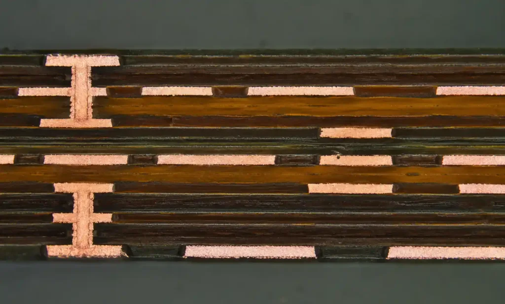
Stack-up architecture matters significantly. For multilayer flex circuits, positioning copper layers symmetrically around the neutral axis minimizes stress during flexing. In a 4-layer construction, placing heavier copper (70μm/2 oz) on outer layers and lighter copper (18μm/½ oz) on inner layers creates asymmetric stress distribution that accelerates copper cracking. Instead, we specify uniform copper weight across all layers or place heavier copper on inner layers for static portions.
Adhesiveless construction has become our default specification for dynamic flex applications. Traditional acrylic adhesives add 15-25μm per bond layer and create stress concentration points. Cast polyimide construction eliminates these adhesive layers, improving flex life by 40-60% while reducing overall thickness by 30-50μm in typical 2-layer constructions.
Conductor Thickness and Trace Design
Copper weight selection directly impacts both electrical performance and mechanical reliability. The industry standard ½ oz (18μm) copper provides adequate current carrying capacity for most signal applications while maintaining good flexibility. However, for power distribution in battery management systems, we’ve found that transitioning to 1 oz (35μm) copper in static sections while maintaining ½ oz in flex regions provides optimal performance.
Current carrying capacity scales with trace width and copper thickness, but the relationship isn’t linear. A 0.3mm wide trace in ½ oz copper safely carries approximately 1.2A with 10°C temperature rise in free air. Doubling to 1 oz copper increases capacity to 1.8A (only 50% increase), while doubling trace width to 0.6mm increases capacity to 2.1A (75% increase). This demonstrates that width adjustments often prove more effective than thickness increases for current capacity.
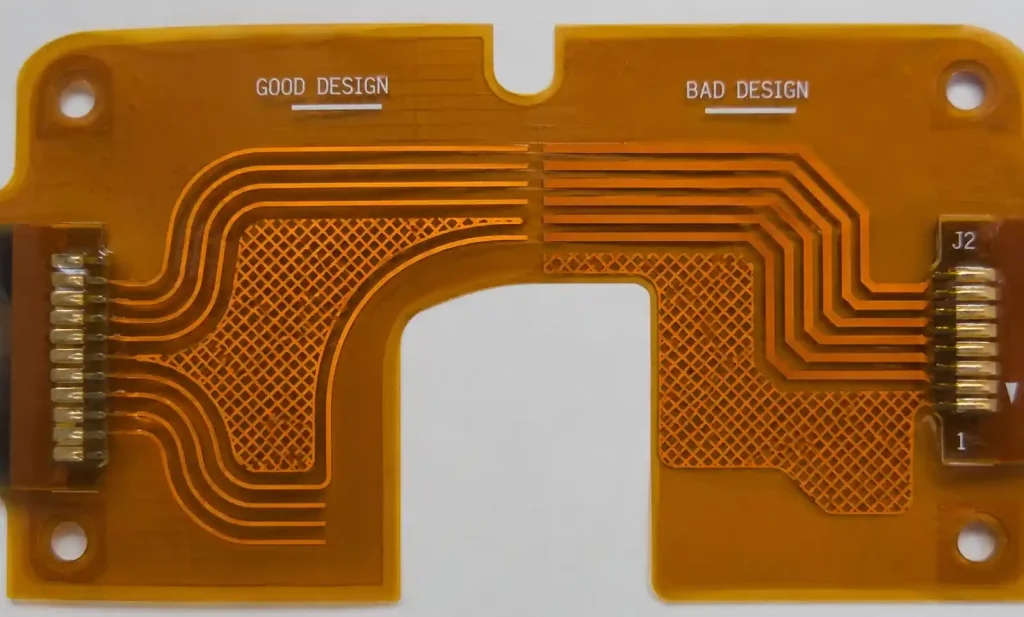
Trace geometry in flex regions requires special attention. We mandate curved traces (radius ≥5× trace width) rather than 90° angles in areas subject to flexing. Sharp corners create stress concentration points that initiate copper cracking. In our accelerated life testing, circuits with radiused traces in flex regions achieved 8× longer flex life compared to designs with right-angle routing.
Cross-hatching copper fills instead of solid pours in flex regions improves flexibility while maintaining electrical functionality. We specify 50% copper density with hatched patterns for ground planes in dynamic flex areas, compared to 90%+ solid pours in static regions.
Stiffener Requirements and Placement
Stiffener selection represents a critical but often overlooked specification. Stiffeners serve three primary functions: providing mechanical support for connectors, enabling automated assembly handling, and protecting circuits during installation. Incorrect stiffener specification causes 20-30% of our customer returns during prototype phases.
Polyimide stiffeners (0.1-0.4mm thickness) maintain flexibility while providing local rigidity. We specify these for areas requiring modest reinforcement, such as supporting lightweight ZIF connectors or creating defined bend regions. FR-4 stiffeners (0.2-1.6mm thickness) deliver rigid support for heavy connectors but create abrupt flexibility transitions that require careful design of transition zones.
| Stiffener Type | Thickness Range | Applications | Relative Cost |
|---|---|---|---|
| Polyimide film | 0.1-0.4mm | Light support, defined bend zones | 1.0× |
| FR-4 rigid | 0.2-1.6mm | Connector support, component mounting | 0.8× |
| Stainless steel | 0.05-0.2mm | EMI shielding, heat dissipation | 1.8-2.5× |
| Adhesive film only | 0.05-0.1mm | Minimal support, adhesive backing | 0.3× |
Stiffener transition zones require specific design rules. We maintain a minimum 3mm gap between the stiffener edge and the beginning of the flex region, with the stiffener edge chamfered or radiused. Abrupt stiffener terminations create stress risers that initiate delamination—in our testing, chamfered edges extend flex life by 2-3× compared to square-cut stiffeners placed immediately adjacent to flex regions.
Adhesive selection for stiffener attachment impacts performance. Pressure-sensitive adhesives (PSA) enable rework but can creep under thermal cycling. Thermosetting adhesives like acrylic provide superior bond strength for permanent assemblies. For applications experiencing >125°C, we specify high-temperature PSAs or thermosetting epoxies to prevent delamination.
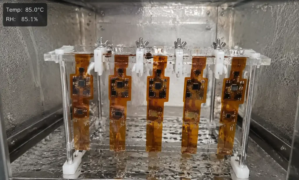
Environmental Resistance Specifications
Environmental specifications define the extremes your flexible PCB must survive. Standard consumer-grade flex circuits typically specify -20°C to +85°C operating range with 85% relative humidity. However, our industrial and automotive projects routinely require -40°C to +125°C with exposure to chemicals, UV radiation, and mechanical contamination.
Chemical resistance varies dramatically by substrate material. Polyimide resists most solvents, oils, and cleaning agents, but shows limited resistance to strong bases. In alkaline battery applications, we’ve documented polyimide degradation when exposed to potassium hydroxide leakage. For such applications, LCP substrates provide superior resistance.
Conformal coating selection substantially improves environmental resistance. Acrylic coatings provide moisture resistance and limited chemical protection at low cost. Polyurethane coatings offer excellent abrasion resistance and flexibility. For harsh environments, we specify parylene coating—a vapor-deposited polymer that conformally coats at 5-30μm thickness, providing exceptional moisture barrier properties and chemical resistance without significantly impacting flexibility.
UV exposure considerations often get overlooked. Standard polyimide yellows and becomes brittle after prolonged UV exposure. For outdoor applications or automotive dashboard integration, we specify UV-stabilized polyimide formulations or add UV-protective overlays. These add 8-12% to material costs but prevent embrittlement that would otherwise occur within 12-18 months of outdoor exposure.
Salt spray resistance proves critical for marine and coastal applications. We specify ENIG (Electroless Nickel Immersion Gold) surface finish instead of HASL (Hot Air Solder Leveling) for circuits exposed to salt spray environments. ENIG provides superior corrosion resistance, with circuits passing 500+ hours of salt spray testing per ASTM B117 compared to <100 hours for HASL-finished circuits.
Manufacturing Capabilities and Lead Times
Manufacturer capability assessment prevents costly redesigns. Not all flex PCB manufacturers offer equivalent capabilities—process limitations often surface only after prototype delivery. We maintain a pre-qualified manufacturer list segmented by capability tier after experiencing multiple project delays from manufacturers accepting specifications they couldn’t reliably produce.
Critical capability verification points include:
Minimum feature sizes: Standard flex manufacturers reliably produce 100μm (4 mil) traces/spaces. Advanced manufacturers handle 75μm (3 mil) with 95%+ yield. Specifications below 75μm require specialized manufacturers and increase costs by 40-60%. We’ve found that pushing beyond a manufacturer’s demonstrated capability results in yield loss that extends lead times by 2-4 weeks.
Via technology determines routing density. Standard flex supports 300μm diameter through-holes. Blind and buried vias require sequential lamination, limiting manufacturer selection and adding 15-25% to costs. Laser-drilled microvias (<150μm) enable HDI flex designs but restrict your manufacturer pool to perhaps 20-30 suppliers globally with proven capability.
Registration tolerance impacts design rules. Standard flex manufacturing maintains ±75μm (±3 mil) layer-to-layer registration. This affects minimum annular ring specifications and via-in-pad feasibility. We specify 125μm (5 mil) minimum annular ring for through-holes and 75μm (3 mil) for blind vias, accounting for worst-case registration tolerance.
Lead time variations span dramatically—from 3-5 days for simple prototypes from specialized quick-turn suppliers to 8-12 weeks for complex multilayer constructions requiring specialized materials. Our typical industrial projects budget 6-8 weeks for first article flex circuits including material procurement.
Cost Drivers and Budget Optimization
Flexible PCB costs typically range from 2-5× equivalent rigid PCB costs, driven by specialized materials, lower panel utilization, and manual processing steps. Understanding cost drivers enables strategic optimization without compromising performance.
Primary cost drivers ranked by impact:
Material selection represents 40-50% of total cost. Switching from polyimide to polyester reduces material costs by 50-60% where thermal requirements permit. Coverlay material selection offers similar optimization—polyimide coverlay costs 2-3× more than photoimageable coverlay (solder mask), though coverlay provides superior flexibility and reliability.
Panel utilization dramatically impacts unit costs. Flexible circuits waste more panel area than rigid PCBs due to irregular shapes. We collaborate with manufacturers during layout optimization to improve utilization from typical 40-50% to 60-70%, reducing unit costs by 20-30% without any technical changes.
| Cost Factor | Impact on Total Cost | Optimization Strategy |
|---|---|---|
| Base material | 40-50% | Consider PET where thermal permits |
| Layer count | 20-30% | Minimize layers through HDI techniques |
| Panel utilization | 15-25% | Optimize layout with manufacturer |
| Feature sizes | 10-15% | Avoid pushing minimum capabilities |
| Surface finish | 5-8% | Match finish to application needs |
Stiffener choices significantly impact assembly costs even if material costs seem modest. Circuits requiring multiple stiffener types or complex stiffener geometries increase labor costs by 30-50%. We consolidate stiffener specifications where possible, sometimes accepting slight performance compromise for substantial cost reduction.
Volume breaks occur at different thresholds than rigid PCBs. Flexible PCB manufacturing shows limited economy of scale until reaching 500-1,000 units due to setup-intensive processes. For low-volume applications, we evaluate rigid-flex alternatives that might offer better cost structure below 200 units.
NRE (Non-Recurring Engineering) costs for flex circuits include tooling for coverlay, stiffeners, and specialized testing fixtures. Budget $800-2,500 for standard designs and $3,000-8,000 for complex constructions with multiple stiffeners or specialized testing requirements. These costs amortize quickly above 500 units but significantly impact prototype economics.
Conclusion
Selecting the optimal flexible PCB requires balancing ten interconnected factors—from substrate material through environmental resistance to manufacturing capabilities. The key insight from our experience: start with application requirements (operating temperature, flex cycles, environment) to establish baseline material and construction specifications, then optimize panel utilization and feature sizes within manufacturer capabilities to control costs.
For most new projects, we recommend this decision sequence: define environmental extremes first (temperature, chemicals, moisture), establish flex cycle requirements second (static, occasional, or dynamic), select appropriate base material third (polyimide vs polyester vs LCP), then configure layer count and copper weight to meet electrical requirements while maintaining required flexibility. This sequence prevents the common mistake of optimizing cost first, only to discover the resulting specification can’t survive the application environment.
The flexible PCB industry continues evolving rapidly. Stretchable circuits, embedded components in flex substrates, and hybrid rigid-flex-stretchable constructions represent emerging capabilities worth monitoring for future designs. However, mastering these ten fundamental factors will guide 95% of current flexible PCB selection decisions toward successful outcomes.